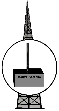
Active antenna 1 to 20dB, 1-30 MHz range.
by
Rodney A. Kreuter
and
Tony van Roon
"When fate or nasty neighbors prevent you from stringing a long-wire receiving
antenna, you'll find that this pocket-size antenna will give the same, or even better, reception. This "Active Antenna"
is cheap to build" and has a range of 1 to 30Mhz at between 14 and 20dB gain."
For conventional all-frequency short-wave reception, the general rule is
"the longer the antennal the stronger the received signal." Unfortunately, between nasty neighbors, restrictive housing
rules, and real-estate plots not much larger than a postage stamp, short-wave antennae often turn out to be a few feet
of wire thrown out of the window--rather than the 130 feet of long-wire antennal we would really like to string between
two 50-foot towers.
Fortunately, there is a convenient alternative to the long-wire antenna, and that's an active antenna; which
basically consists of a very short antenna and a high-gain amplifier. My own unit has been in operation successfully for
almost a decade. It works satisfactory.
The concept of a active antenna is fairly simple. Since the antenna is physically small, it doesn't intercept as much
energy as a larger antenna, so we simply use a built-in RF amplifier to make up for the apparent signal "loss." Also,
the amplifier provides impedance matching, because most receivers are designed to work with a 50-ohm antenna.
Active antennas can be built for any frequency range, but they are more commonly used from VLF (10KHz or so) to about
30MHz. The reason for that is because full-size antennas for those frequencies are often much too long for the available
space. At higher frequencies, it is quite easy to design a relatively small high-gain antenna.
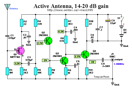
The active antenna shown below (Fig. 1), provides 14-20dB gain at the popular short-wave and radio-amateur frequencies of
1-30MHz. As you would expect, the lower the frequency the greater the gain. A gain of 20dB is typical from 1-18 MHz,
decreasing to 14dB at 30MHz.
Circuit Design:
Because antennas that are much shorter than 1/4 wavelength present a very small and highly reactive impedance that is
dependent on the received frequency, no attempt was made to match the antenna's impedance--it would prove too difficult
and frustrating to match impedances over a decade of frequency coverage. Instead, the input stage (Q1) is an JFET
source-follower, whose high-impedance input successfully bridges the antenna's characteristics at any frequency.
Although many different types of JFET's may be used--such as the MPF102, NTE451, or the 2N4416--bear in mind that the
overall high-frequency response is set by the characteristics of the JFET amplifier.
Transistor Q2 is used as an emitter-follower to provide a high-impedance load for Q1, but more importantly, it provides
a low drive impedance for common-emitter amplifier Q3, which provides all of the amplifier's voltage gain. The
most important parameter of Q3 is fT, the high-frequency cut-off, which should be in
the range of 200-400 MHz. A 2N3904, or a 2N2222 works well for Q3.
The most important of Q3's circuit parameters is the voltage drop across R8: The greater the drop, the greater the
gain. However, the passband decreases as Q3's gain is increase.
Transistor Q4 transform Q3's relatively moderate output impedance into a low impedance, thereby providing sufficient
drive for a receiver's 50-ohm antenna-input impedance.
 Parts List and other components:
Semiconductors:
      Q1 = MPF102, JFET. (2N4416, NTE451, ECG451, etc.)
Q2,Q3,Q4 = 2N3904, NPN transistor

Resistors:
All Resistors are 5%, 1/4-watt
    R1 = 1 MegOhm           R5 = 10K
R2,R10 = 22 ohm          R6,R9 = 1K
R3,R11 = 2K2                R7 = 3K3
    R4 = 22K                R8 = 470 ohm

Capacitors (rated at least 16V for a 9V supply):
   C1,C3 = 470pF
C2,C5,C6 = 0.01uF  (10nF/103)
      C4 = 0.001uF (1nF/104)
   C7,C9 = 0.1uF   (100nF/102)
      C8 = 22uF/16V, electrolytic

Miscellaneous Parts & Materials:
  B1 = 9-volt Alkaline battery
  S1 = SPST on-off switch
  J1 = Jack to match (your) receiver cable
ANT1 = Telescoping whip antenna (screw mount), wire, brass rod (about 12")
MISC = PCB materials, enclosure, battery holder, 9V battery snap, etc.
If you wish to purchase a parts-only kit (NO pcb), click here: [AA-8 parts-only KIT]
The antenna can be almost anything; a long piece of wire, a brass welding rod, or a telescopic antenna that was salvaged
from an old radio. Telescopic replacement antennas for transistor radios are also available from most retail
electronic-parts distributors and suppliers.
Construction:
The amplifier for the prototype unit uses a printed-circuit board (see below). The amplifier can be assembled on a
perforated wiring board (vero board), but because there is some sensitivity to the parts layout, we strongly
suggest that you create a printed circuit board (PCB) for best results.

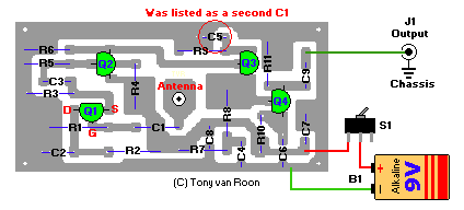
The parts-placement diagram is shown in Fig. 2. Take note that although the battery's negative (ground) lead is
returned to the PC board, output-jack J1 has a connection to the cabinet ground. The ground connection between the
PC board and the cabinet is made through the metal standoffs or spacers that are used to mount the PC board in the
enclosure. Do *NOT* substitute plastic standoffs or spacers because they won't provide a ground connection between the
PC board, the cabinet, and J1. If you decide to use a plastic cabinet to house the amplifier, make certain that J1's
ground connection is returned to the ground foil running around the outer-edge of the PC-board.
A telescopic antenna mounts in the center of the PC board. From the foil side of the board, pass its mounting screw
through the hole in the PC board and then solder the head of the screw to its foil pad. For both insulation and
support, we use a plastic or rubber grommet between the antenna and the hole in the cabinet's cover through which the
antenna passes. In a pinch, several turns of a good-quality plastic tape wrapped around the antenna's shaft can be
substituted for the rubber grommet.
If you decide to make provisions for a wire antenna, install a 5-way binding post on the cabinet. Then, be sure to
connect a short length of wire between the antenna's foil pad and the binding post.
Modifications:
If you are interested in a smaller frequency range than 1-30MHz, resistor R1 can be replaced with an LC tank circuit
tuned to the center of the desired range. The LC circuit will also improve the rejection of signals outside your range
of interest, but remember that it won't improve the gain of the amplifier.
If your particular interest is the very-low frequencies (VLF), the amplifier's low-frequency response can be improved by
increasing the values of capacitors C1 and C3. (You'll have to experiment with the values.)
Although a 9-volt battery is the recommended power source, the amplifier should work well using 6-15 volts. The inside
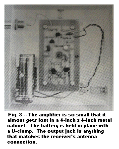
of the cabinet of the completed prototype, using a 9-volt battery as the power supply, is shown in Fig. 3.
Troubleshooting:
Circuit voltages for a 9-volt power supply are shown in the schematic diagram Fig. 1. If the voltages in your unit
differ more than 20% from those in the schematic, try changing resistor values to get the voltages in their proper
range. For example, if the voltage drop across R8 measures only 0.3 volt, you must decrease R4's value (the exact
value is up to you to figure out) in order to increase Q3's base voltage and collector current.
The only critical voltages are those across R3 and R8. Performance should be fine if they are even close to the
values shown on the schematic diagram.
Since it is almost impossible to measure the voltage from the gate to the source (VGS) of a FET, you can measure the
voltage that is present across R3, because it is the same as VGS. Adjust R3's value accordingly, if the voltage is not
within the range of 0.8-1.2 volts.
Limitations:
Use of this amplifier above 30 MHz is not recommended because of the sharply reduced gain. While operating above 30 MHz
can be accomplished by using tuned circuits in place of the resistive loads, that modification is beyond the scope of
this article.
Take care when handling the FET (Q1). A common belief is that FET's are CMOS devices are safe from static damage after
having been installed in a circuit, or after being mounted to a PC board. Although it is true they are better
protected from static electricity when installed in a circuit, they are still susceptible to damage by static; so
never touch the antenna before discharging yourself to ground by touching some grounded metallic object.
Copyright and Credits:
Source: "R-E Experimenters Handbook", 1990. Copyright © Rodney A.Kreuter,
Tony van Roon, Radio Electronics Magazine, and Gernsback Publications, Inc. 1990. Published by written permission.
(Gernsback Publishing and Radio Electronics are no longer in business). Document updates & modifications, all
diagrams, PCB/Layout drawn by Tony van Roon. Re-posting or taking graphics in any way or form of this project is
expressly prohibited by international copyright laws.
Back to Circuits page
Page, PCB, Layout, Copyright © 1991 - Tony van Roon
Project Copyright © 1990, by Rodney A.Kreuter