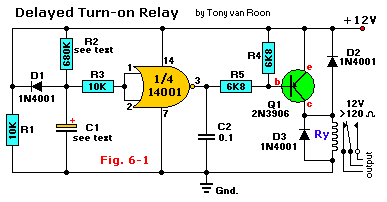
Parts List:
R1,R3 = 10K                     Q1 = 2N3906, or equivalent
   R2 = 680K (see text)        IC1 = CD4001, or equivalent CMOS
R4,R5 = 6K8               D1,D2,D3 = 1N4001, or equivalent
   C1 = see text                Ry = Relay, 12V
   C2 = 0.1uF (100nF), ceramic
This circuit is a delayed turn-on relay driver and can produce time delays for up to several minutes with reasonable
accuracy.
The 14001 (or 4001) CMOS gate here is configured as a simple digital inverter. Its output is fed to the base of a
regular 2N3906 (PNP) transistor, Q1, at the junction of resistor R5 and capacitor C2. The input to IC1 is taken
from the junction of the time-controlled potential divider formed by R2 and C1. Before power is applied to the circuit,
C1 is fully discharged. Therefore, the inverter input is grounded, and its output equals the positive supply rail;
Q1 and RY1 are both off under this circuit condition. When power is applied to the circuit, C1 charges through R2,
and the exponentially rising voltage is applied to the input of the CMOS inverter gate.
After a time delay determined by the RC time constant values of C1 and R2, this voltage rises to the threshold value
of the CMOS inverter gate. The gate's output then falls toward zero volts and drives Q1 and relay Ry 'ON'.
The relay then remains on until power is removed from the circuit. When that occurs, capacitor C1 discharges rapidly
through diode D1 and R1, completing the sequence.
The time delay can be controlled by different values for C1 and R2. The delay is approximately 0.5 seconds for every
uF as value for C1. The delay can further be made variable by replacing R2 with a fixed and a variable resistor
equal to that of the value of R2. Taken the value for R2 of 680K, it would be a combination of 180K for the fixed
resistor in series with a 500K variable trim pot. The fixed resistor is necessary.
Copyright © 2003 - Tony van Roon
ALL RIGHTS RESERVED