"This simple adapter circuit fits inside your FM tuner and lets you tap into hidden
FM transmissions. Although this circuit is from 1989, it still works today and components are readily available."
Re-written by Tony van Roon.
Although still new to some countries, subcarrier transmissions on FM
broadcasts have been made for years. They are referred to as Subsidiary Communications Authorized transmissions or
SCA. They are based on a 67KHz subcarrier that is placed on a station's main FM carrier. It's even possible to have
multiple subcarriers, some carrying digital data and others carrying audio.
So you can receive such broadcasts, we present the SCA Adapter that can be hooked into most FM tuners with a minimum
of fuss. Low in cost, it uses just a few readily available integrated circuits.
Before we describe the Adapter circuit, let's briefly talk about FM-subcarrier transmissions. They have no effect on
standard FM mono and stereo radios. Also, they are fully compatible with all existing FM radios, whether stereo or
mono. In fact, unknown to the great mass of FM listeners, such transmissions have been going on for some time, at
least three decades.
But while all FM radios are presently unaffected, they are capable of picking up the subcarrier transmissions. With the
addition of an adapter such as the one we'll describe here, they will be able to detect the hidden audio signals.
The SCA Adapter prototype was built on a compact printed-circuit board accommodating three low-cost opamps, a
phase-locked loop IC, a 3-terminal regulator, and a handful of resistors and capacitors.
How it Works.
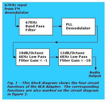
Figure 1 shows a block diagram of our circuit. The 67KHz signal present at the output of the FM detector (in the radio
to be modified) is first fed to a 67KHz bandpass filter, and then to a phase-locked loop (denoted PLL), which covers the
audio on the 67KHZ subcarrier.
The audio output of the PLL is then passed through a low-pass filter, which attenuates frequencies above 6KHz at the
rate of 18 db/octave. Another 12 dB/octave low-pass filter stage completes the conditioning of the signal before it
is passed to an external audio amplifier.
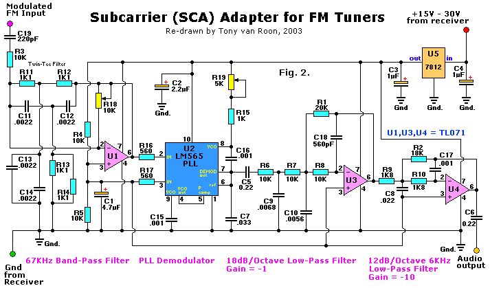
Figure 2 shows the complete circuit. Op-Amp U1 and its associated components comprise the 67KHz bandpass filter.
A twin-T network, comprised of four 1100-ohm resistors and four 0.0022uF capacitors, is connected in the feedback
network of the op-amp.That gives some gain at 67KHz and heavy attenuation for frequencies above and below that
frequency.
An additional passive filter at the input to the twin-T network (containing a 220pF capacitor and a 10,000 ohm resistor)
provides some additional roll-off for frequencies below 67KHz.
In practice, the bandpass-filter action covers a frequency range of about 10KHz above and below the 67KHz center frequency.
Resistor R18 sets the gain of the bandpass-filter stage.
Integrated-circuit U2 is a National LM565 Phase-Locked Loop that demodulates the 67KHz frequency-modulated (FM) signal
from U1. The LM565 PLL consists of a voltage-controlled oscillator (VCO) set to 67 KHz, and a comparator that compares
the incoming frequency-modulated 67KHz signal at pin 2 with the VCO signal fed into pin 5.
The output of the comparator represents the phase difference between the incoming signal and the VCO signal, and is
therefore the audio modulated by the subcarrier. Treble de-emphasis of 150uS is provided by a 0.033uF capacitor (at
pin 7).
Parts List for the SCA Adapter
Semiconductors:                             C18 = 560pF, Polystyrene
U1,U3,U4 = TL071, FET OpAmp                 C19 = 220pF, Ceramic disc
      U2 = LM565, Phase-Locked-Loop
      U5 = LM7812, 12V Regulator            Resistors:
                                           (All resistors are 1/4W, 5% precision
Capacitors:                                 units unless otherwise noted.)
     C1 = 4.7uF/16V, electrolytic             R1 = 20K, 2% precision
     C2 = 2.2uF/16V, electrolytic             R2 = 18K
     C3 = 1uF/16V, electrolytic		   R3-R8 = 10K
     C4 = 1uF/35V, electrolytic		  R9,R10 = 1K8
  C5,C6 = .22uF, metalized Polyester     R11-R14 = 1100 ohm, 2% precision
     C7 = .033uF, metalized Polyester        R15 = 1K
     C8 = .022uF, metalized Polyester    R16,R17 = 560
     C9 = .0068uF, metalized Polyester       R18 = 10K, miniature vertical
    C10 = .0056uF, metalized Polyester                  trimmer potentiometer
C11-C14 = .0022uF, metalized Polyester       R19 = 5K, miniature vertical
C15-C17 = .001uF, metalized Polyester                  trimmer potentiometer

Note: A complete Kit and PCB for this project will be available shortly.
The free running VCO frequency is determined by the 0.001uF capacitor at pin 9, and the resistance between the positive
rail and pin 8 (100-ohms in series with R19). Variable resistor R19 adjusts the oscillator frequency (also known as
the "center frequency") so that the incoming signal is within the lock range of the PLL.
To minimize noise in the demodulated output, it is important to reduce the lock range of the PLL to a minimum. That is
achieved by shorting pins 6 and 7 together. To a lesser extend, the lock range--and therefore the noise output--becomes
smaller for lower input signals, so we keep the input signal as low as possible without affecting the PLL's operation.
Following U2 is the 18-dB/octave filter containing U3, which has a gain of one for the desired signal frequencies.
The filter is followed by the final stage, U4, which has a gain of 10.
The adapter is ideally powered from the tuner or receiver it is built into, so we had to make its input-voltage
requirements non-critical. The solution is to use a 12-volt, 3-terminal regulator that enables the circuit to be
powered from any +15 to +30-volt supply.
The three op-amp IC's and the PLL are all biased to half the supply voltage by a voltage divider consisting of two
10,000 ohm resistors, which is decoupled by a 4.7uF capacitor. The center of the voltage divider is connected to pin 3
of each op-amp and the PLL.
PCB Assembly.
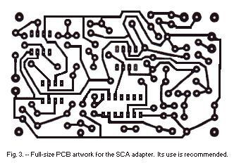
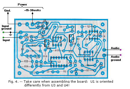
The printed-circuit board for the project (see Fig. 3) measures just 3-5/8x2-1/4-inch and will help ease assembly if
made. Point-to-point assembly can be used but will be a bit difficult to perform accurately.
No special points need to be watched when installing the parts on the board except that component polarities must be
correct (see Fig. 4). Note also that U1 has a different orientation to U2, U3, and U4.
When assembly and soldering are finished, check your work carefully and then connect a DC supply of between 15 and 30
volts. Now check the voltage at the output of the 3-terminal regulator, at pin 7 of the TL071 op-amps, and at pin 10
of the PLL. In each case, the reading should be close to 12-volts. The voltage at pins 3 and 6 of each op-amp, and
pin 3 of the PLL, should be close to 6-volts DC.
If everything is okay, you are ready to install the Adapter in your FM tuner of stereo receiver.
Finding the Signal.
Here comes the tricky part. Ideally, you need access to the circuit diagram of your tuner or receiver. Next, you
need to identify a positive DC-supply rail of between +15 and +30-volts. Then, you need to find the output of
the FM demodulator of your receiver or tuner.
In a stereo tuner, that comes before the multiplex decoder and treble de-emphasis networks. In a mono tuner, you must
identify the demodulator output before the de-emphasis. After the-emphasis, the 67KHz signal will be non-existent.
Most medium-priced tuners use two IC's to do most FM-signal processing. They are the IF amp and detector IC, followed
by a multiplex (MPX) decoder IC. The most convenient point to pick off the 67KHz signal is at the input to the
MPX decoder.
 Setting Up.
Having found the signal and made the necessary connections from the Adapter to your tuner, the setup procedure is
relatively simple. First, make sure that R18 is set so that its wiper is turned toward the LM565. That will provide
maximum signal. Now adjust R19 so that there is an audio signal. Find the extreme settings of R19 where the audio
signal drops out, then set R19 between the two extremes.
Resistor R18 is used to minimize noise from the audio signal when the FM signal level is poor. Adjust the trimmer
until the sound becomes distorted and then back off the adjustment until the distortion is no longer audible. If you
have a strong FM signal, adjustment of R18 will have no effect on the noise level, and so it should be left at its
maximum-resistance setting.
Copyright and Credits:
Source: "Hands-on Electronics" magazine, January 1989. Copyright © John Clarke, Leo
Simpson, and publisher Gernsback Publications, Inc. 1989. Published with permission from Gernsback. (Gernsback
Publishing no longer in business since Jan. 2000).
Document updates & modifications, all diagrams, PCB/Layout drawn by Tony van Roon.
Re-posting or taking graphics in any way or form of this project is expressly prohibited by international
copyright laws.
Back to Circuits page
Page Copyright © 1995 - Tony van Roon
Project Copyright ©John Clarke and Leo Simpson