Transistor Tutorial
Part 11:
"All About Transistors: FET's"
Transistor Tutorial, Part 11: "All About Transistors: FET's"
"The lowly transistor evolved from bipolar to JFET to MOSFET to CMOS--which
today forms the basis of many industrial and commercial products. by Robert A. Young."
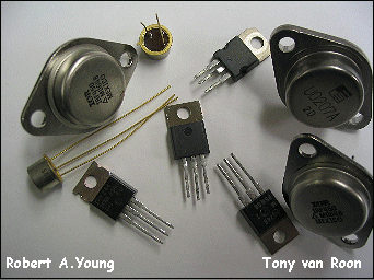
Original article by Robert A. Young.
Rewritten, updated, and modified by Tony van Roon
It
may seem hard to believe, but it was not too long ago that bipolar transistors began to replace vacuum tubes in
mainstream electronics design. Low power, small size, and durability were only a few of the characteristics that
propelled those little globs of silicon into the forefront of electronics. However, tube circuits didn't abruptly or
magically disappear when transistors hit the scene in part because bipolar transistors have a low input impedance,
are noisy, and must be safeguarded against thermal runaway. On the contrary. Vacuum tubes today (2008) are coming
back! Even new manufacturers popped up to make these tubes. From where the popularity? Well, mainly the music
industry. Nothing beats a well designed guitar tube amplifier. The warm and robust sound from a tube-amp cannot be
matched by a transistor version of the same kind. Then there is nostalgia. Our young electronics hobbyists today are
curious how such tube amp works and so they built it. Good for them. This generation have my full attention and I
will help them where and however I can! It has been though to keep the electronics hobby alive since the latter part
of the 90's. Solid electronics magazines, like Radio Electronics, the same my father was reading, went under and
disappeared together with Popular Electronics, Hobby Electronics, and many other to give way to the Internet. Now,
finally after more than a decade, they seem to trickle back. The most popular being Elector Magazine and
Nuts and Volts Magazine. Fantastic!
When the Field-Effect Transistor (FET) was introduced, it overcame many of the shortcomings of bipolar units. In fact,
it combined many of the advantages of bipolar transistors and vacuum tubes into a single package.
Thus, several devices that were traditionally vacuum-tube based began to show up in transistorized form. However,
before we take a look at the FET, let's take a look again at its forerunner, the bipolar transistor.
 Bipolar Transistors:
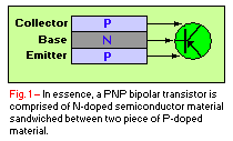
Figure 1 shows the composition of a PNP bipolar transistor. As shown, N-doped material is
sandwiched between two pieces of P-doped material. The base is comprised of the N-type material, while the collector and
emitter of the transistor is made up of P-type material.
In order for a PNP transistor to conduct, its collector must be made more negative than its base, and its base more
negative than its emitter. That condition is called "forward biasing." Note that the potential (or voltage) polarity
is not specified. That's because bipolar transistors can be operated from either a negative of positive source, as
long as they are properly biased.
Current flow between the base-emitter junction causes current flow in the emitter-collector junction. NPN transistors
operate in the exact same manner except current flow is in the opposite direction, and their bias voltages are reversed
as well; e.g., for an NPN transistor to operate, its collector must be more positive than its base, and its base more
positive than its emitter terminal.
It doesn't take a deep understanding of transistor physics to see that the two separate junctions (base-emitter and
collector-base) behave much as two diodes. The input impedance of a bipolar transistor is consequently very much the
same as a forward-biased diode (it's low). That's one of the main reasons that the introduction of the transistor did
not totally do away with vacuum tubes. Since vacuum tubes have an inherently high input impedance, it was much easier
to use them than to devise additional circuits to provide bipolar transistors with similar desirable characteristics.
Enter the FET:
While bipolar transistors are basically current amplifiers, field-effect transistors (FET's)--which are unipolar rather
than bipolar devices--are voltage amplifiers. FET's have certain properties that are superior to those of bipolar
transistors. For instance, voltage rather than current with respect to voltage at specified bias levels, current
change that is inversely (rather than directly) proportional to temperature, as well as faster switching speeds and
thus higher cut-off frequencies. Despite those advantages, the FET has not replaced bipolar transistors in all applications.
There are two major classes of GET: the junction field-effect transistor or JFET, and the metal-oxide semiconductor
field-effect transistor or MOSFET (which is sometimes called an "insulated-gate FET" or "IGFET").
FET's are further categorized by channel type (N or P), and as being normally on (depletion) or normally off
(enhancement).
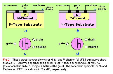 Cross sectional views of both N- and P-channel JFET's are shown in Figs. 2A and 2B,
respectively. As shown in Fig. 2A, an N-channel FET is formed by embedding (channeling)
N-type material in a P-type substrate. The P-type substrate is referred to as the "gate", while the two regions of
embedded N-type material are designated the "source" and the "drain". Respectively speaking, the source, gate, and
drain of a FET are analogous to the collector, base, and emitter of a bipolar transistor.
Cross sectional views of both N- and P-channel JFET's are shown in Figs. 2A and 2B,
respectively. As shown in Fig. 2A, an N-channel FET is formed by embedding (channeling)
N-type material in a P-type substrate. The P-type substrate is referred to as the "gate", while the two regions of
embedded N-type material are designated the "source" and the "drain". Respectively speaking, the source, gate, and
drain of a FET are analogous to the collector, base, and emitter of a bipolar transistor.
Source and drain terminals are formed directly on the N-channel material an the gate terminal is formed on the P-type
area. The symmetrical construction of the JFET permits the drain and source to be interchanged, if necessary. The
schematic symbols for both N- and P-channel FET's are shown in Figs. 2C and 2D, respectively.
FET Operation:
There are two interrelated factors that control the performance of a FET (i.e., current flow through the embedded
channel): the voltage between the gate and source (Vgs); and the voltage from drain-to-source (Vds).
If the gate-to-source voltage is at ground (zero volts) with he drain connected to a positive voltage and the source
tied to ground, the electron shortage in the channel restricts the amount of current that can flow through the channel.
The only way to increase current flow is to increase the drain-to-source voltage.
Let's take a look at what happens when a signal source is connected to the gate of a FET and a positive voltage is
applied to the drain (refer to Fig. 2A). If a positive voltage is applied to the drain and a negative voltage is
applied to the source with the gate terminal open, a drain current flows.
When the gate is biased negative with respect to the source, the PN junction is reverse biased, which causes a
depletion region to form. Because the N-channel is more lightly doped that the P-type gate material, the depletion
region penetrates into the N-channel. The depletion region, which behaves like an insulator, causes the N-channel to
narrow, increasing the channel resistance. If the gate bias is made even more negative, the drain current is
eventually cut off completely. The voltage at which that happens is called the "pinch-off" or "gate cut-off" voltage.
On the other hand, as the gate bias is made more positive, the depletion region shrinks, reducing the source-to-drain
resistance, which in turn causes an increase in current flow through the channel.
For a P-channel JFET (refer to Fig. 2B), if a negative voltage is applied to the drain and a positive voltage to the
source with the gate terminal open, a current flows through the channel. When the gate is made positive with respect
to the source, the depletion region begins to increase, narrowing the P-channel and causing the channel's resistance to
increase. The increased resistance of the channel reduces current flow. If gate bias is made more positive and
reaches the pinch-off or gate cur-off voltage, current flow is completely choked off.
On the other hand, as the bias becomes more negative, the depletion region shrinks, reducing the source-to-drain
resistance, increasing current flow. Thus, the gate actually controls current flow through the channel.
The gate-to-source junction of a JFET has the characteristics of a silicon diode; that is, when reverse biased, gate
leakage current is in the thousands of microamps at room temperature. Actual gate-signal current is only a fraction
of that and the input impedance to the gate is typically 1000 megohms at low frequencies. The gate junction is
effectively shunted by a capacitance of a few picoFarads, so its input impedance falls as the frequency increases.
If the gate-to-source junction of the JFET is forward biased, it conducts like a normal silicon diode, and if it is
severely reverse biased, it avalanches like a Zener diode. Neither condition will harm the JFET if the gate current
is limited to specified levels..
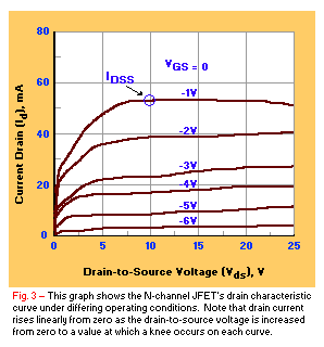 Figure 3 is a graph showing some JFET-drain characteristic curves (in this case, for an
N-channel JFET). It can be seen from that graph that for each value of gate-to-source voltage, drain current rises
linearly from zero as the drain-to-source voltage is in creased from zero to a value at which a knee occurs on each
curve. In addition, drain current remains virtually constant as the drain-to-source voltage is increased beyond the
knee.
Figure 3 is a graph showing some JFET-drain characteristic curves (in this case, for an
N-channel JFET). It can be seen from that graph that for each value of gate-to-source voltage, drain current rises
linearly from zero as the drain-to-source voltage is in creased from zero to a value at which a knee occurs on each
curve. In addition, drain current remains virtually constant as the drain-to-source voltage is increased beyond the
knee.
Therefore, when the drain-to-source voltage for any of the gate-to-source voltage curves is below its knee value, the
drain-to-source terminals of the JFET act like a voltage-variable resistor whose value is determined by the applied
gate-to-source voltage. The drain-to-source resistance (Rds) can be varied from several hundred ohms to
several thousand megohms. That characteristic permits the JFET to be used as a voltage-controlled switch. The drain's
characteristic curve also shows that when the drain-to-source voltage is above the knee value, the drain current is
dictated primarily by the gate-to-source voltage, and is essentially independent from the drain-to-source voltage.
That allows the JFET to function as a voltage-controlled current generator.
The gain of the JFET is specified as a transconductance (Gm); e.g., the rate of drain-current change with
respect to gate voltage. A gain of 5-mA-per-volt indicates that a variation of 1 volt at the gate produces a 5-mA
change in drain current.
Note that transistor structures back in Fig. 2A and Fig. 2B, are complimentary to each other: e.g., in Fig. 2A the
channel is comprised of N-type material and the gate and the substrate are composed of P-type material, but in Fig. 2B
the channel is comprised of P-type material and the gate and the substrate are composed of N-type material. Thus, the
bias voltages for N-channel and P-channel JFET's are opposite each other.
 MOSFET's:
The metal-oxide semiconductor field-effect transistor (MOSFET), developed as an improved JFET, had become one of the
most important forms of FET. A MOSFET is almost the same as a JFET, but instead of having a direct connection between
the gate and the substrate, the gate is isolated from the channel by a thin insulator (usually a film of silicon
dioxide).
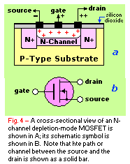
Figure 4A shows a cross-sectional view of an N-channel depletion-mode MOSFET. The gate
of the MOSFET is fully insulated from the adjacent channel--which is the most important difference between it and an
N-type JFET.
When the drain is positive with respect to the source, a current flows even if the applied gate voltage is zero.
However, if the gate is made negative with respect to the substrate, positively charged carriers (holes) induced in
the N-channel combine with the electrons and cause channel resistance to increase. With increasingly negative bias,
the drain current diminishes until the pinch-off voltage is reached, at which point current flow ceases altogether.
However, if the gate is made more positive with respect to the substrate, additional electrons are induced into the
channel increasing the channel current. The schematic symbol for an N-channel depletion-mode MOSFET is shown
if Fig. 4B. The path or channel between the source and the drain is shown as a solid
bar.
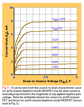 Figure 5 shows the source-to-drain characteristic curve for an N-channel depletion-mode
MOSFET. It can be seen that drain current is inversely proportional to the magnitude of the negative gate voltage.
Note the similarities between the curves for an N-channel depletion-mode MOSFET shown back in Fig. 3.
Figure 5 shows the source-to-drain characteristic curve for an N-channel depletion-mode
MOSFET. It can be seen that drain current is inversely proportional to the magnitude of the negative gate voltage.
Note the similarities between the curves for an N-channel depletion-mode MOSFET shown back in Fig. 3.
 Enhancement MOSFET's:
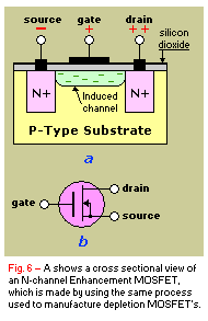
Figure 6 shows a cross sectional view of an N-channel enhancement MOSFET. Enhancement
MOSFET's are manufactured using the same methods used to manufacture depletion MOSFET's. However, the enhancement
MOSFET (see Fig. 6A) does not have the N-doped drain-to-source channel through the P-type substrate as is the case
with the N-channel depletion MOSFET. Therefore, there is no conduction between the drain and the source with no gate
bias applied to the device.
To turn on an enhancement MOSFET, a positive gate voltage is needed. The more positive that gate voltage, the more
electrons are induced into the channel. They can not flow across the outside layer, so they accumulate at the
substrate surface below the gate oxide. When a sufficient number of electrons have accumulated, the P-channel
substrate material is converted into an N-channel, and drain-to-source conduction occurs. The magnitude of the drain
current depends on the channel resistance, but is controlled by the gate voltage. The schematic symbol for an
N-channel MOSFET is shown in Fig. 6B.
In that symbol, the gate does not make direct contact with the channel. The arrow points from the P-type substrate
toward the induced N-type channel, which is shown as a dashed line inside the symbol to indicate an intermittent channel.
Current flow through both types of enhancement MOSFET is proportional to the voltage applied to their gates, and drain
current is directly proportional to the value of any applied positive gate voltage. The P-channel enhancement MOSFET is
made the same way as the N-channel type, except that the direction of the arrow is reversed. In th case of the P-type
enhancement MOSFET, the drain current is directly proportional to any applied negative gate voltage.
The super-high impedance of MOSFET's is a great design advantage, but it makes them susceptible to damage from even
low-energy electro-static discharge (ESD). It doesn't take much static build-up to produce a charge large enough to
puncture the insulating oxide of a MOSFET, destroying the component. For that reason, discrete MOSFET's (as well as
the IC's that incorporate them) are often protected with internal Zener diodes.
In spite of its susceptibility to ESD, the MOSFET comes very close to bridging the gap between vacuum tubes and
semiconductors. Since the gate is totally isolated from the substrate, its input impedance ranges up into hundreds
of megohms.
 CMOS Technology:
An enhancement MOSFET can act as a switch when it is turned on or off by a voltage applied to its gate; N-channel
devices are switched on by a positive gate voltage, but P-channel devices are switched on by a negative gate voltage.
That symmetry of operation is know as a "complementary response", and forms the bases for the CMOS (or complementary
MOS) logic family. That IC family is, of course, sensitive to electrostatic discharge.
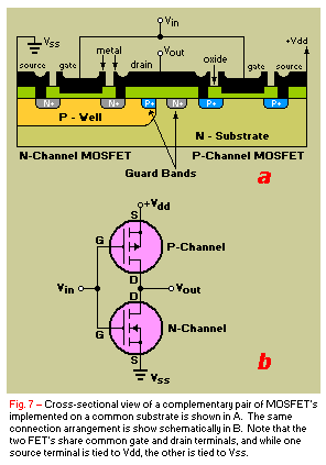
Figure 7A shows a cross-sectional view of a complementary pair of MOSFET's implemented on
a common substrate. The common substrate used for that pair is N-doped silicon material (or "wafer"). Implementing on
a N-channel MOSFET on an N-type substrate requires the defusing or implanting of a P-doped well in the substrate. The
smaller N-type well is then formed in the P-doped region.
Because the substrate is N-doped, fewer steps are required to form the P-channel FET. The P- and N-doped guard bands
are actually N- or P-doped rings formed around the complete FET below the oxide layer.
Two complementary transistors can be connected to form an inverter (the simplest of logic gates). The complementary
arrangement is accomplished by connecting the gates of two MOSFET's together to form a single input Vin
terminal, and taking the output from a common drain. One source (the P-channel) of the complementary pair is connected
to Vdd while the other source terminal is connected to Vss (as shown in Fig. 7B).
With no gate bias applied to the complementary pair, the inverter offers a very high impedance path from the input to
ground, therefore the output voltage rises to Vdd. When the input voltage is high (logical 1), the
situation is reversed, the P-channel device is cutoff, and the N-channel unit is turned on, so the input voltage drops
to zero. Thus, a logical-high input gives a logical-low output, and vice versa. In either logic state, one MOSFET is
on, while the other is off.
Copyright and Credits:
© Original author Robert A. Young. Popular Electronic Magazine, May 1994.
Published by Gernsback Publishing. (Hugo Gernsback Publishing is (sadly) out of business since January 2000).
All graphics, photo's prints, modifications and updates © 2006, Tony van Roon
Re-posting or taking graphics in any way or form from this website or of this project is expressly prohibited by
international copyright © laws.
Continue with Transistor Tutorial: Part 12,
"Design Oscillator Circuits" or go back to Part 10
Copyright © 2006 - Tony van Roon, VA3AVR
Last updated: December 18, 2009