"Learn about audio power amplifiers and apply this knowledge to your circuits
designs and experiments."
An audio power amplifier can boost weak signals from a tuner, CD player, or tape deck to fill a room with sound. This
article focuses on the operating principles and circuitry of low-frequency power amplifiers based on the bipolar junction
transistor (BJT). Other articles in this series have discussed multivibrators, oscillators, audio preamplifiers, and
tone-control circuits, all based on the BJT.
Power Amplifier Basics:
A transistorized audio power amplifier converts the medium-level, medium-impedance AC signal into a high-level,
amplified signal that can drive a low-impedance audio transducer such as a speaker. A properly designed power
amplifier will do this with minimal signal distortion.
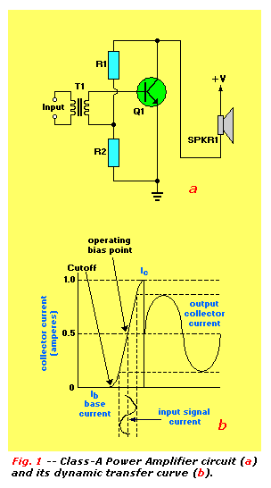
Audio can be amplified with one or more power transistors in either of three configurations: Class A, Class B, and
Class AB. Figure 1-a shows a single BJT Class A amplifier in a common-emitter
configuration with a speaker as its collector load. A Class A amplifier can be identified by the way its input base
is biased.
Fig. 1-a shows that BJT Q1's collector current has a quiescent value that
is about halfway between the zero bias and cutoff positions. (The quiescent value is that value of transistor bias
at which the negative- and positive-going AC input signals are zero.) This bias permits the positive and negative
swings of the output collector AC current to reach their highest values without distortion. If the AC and DC
impedances of the speaker load are equal, the collector voltage will assume a quiescent value that is about half the
supply voltage.
The Class A circuit amplifies audio output with minimum distortion, but transistor Q1 consumes current
continuously--even in the quiescent state--giving it low efficiency. Amplifier efficiency is defined as the
ratio of AC power input to the load divided by the DC power consumed by the circuit.
At maximum output power, the efficiency of a typical Class A amplifier is only 40%, about 10% less than its
theoretical 50% maximum. However, its efficiency falls to about 4% at one-tenth of its maximum output power level.
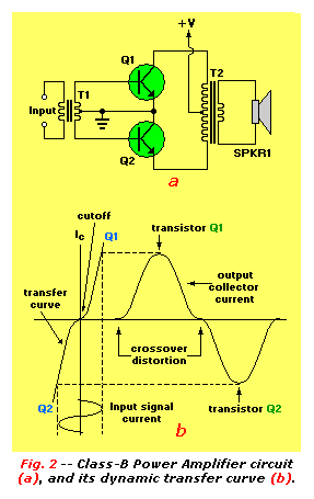
A typical Class B amplifier is shown in Fig. 2-a. It has a pair of BJTs, Q1 and
Q2, operating 180° out-of-phase driving a common output load, in this example another speaker. In this topology,
the BJTs operated as common-emitter amplifiers drive the speaker through push-pull transformer T2. A phase-splitting
transformer T1, provides the input drives for Q1 and Q2 180° out-of-phase.
The outstanding characteristic of any Class B amplifier is that both transistors are biased off under quiescent
conditions because they are operated without base bias. As a result, the amplifier draws almost no quiescent current.
This gives it an efficiency that approaches 79% under all operating conditions. In Fig. 2-b,
neither Q1 nor Q2 conducts until the input drive signal exceeds the base emitter zero-crossing voltage of the
transistor. This occurs at about 600 millivolts for a typical power transistor.
The major disadvantage of the Class B amplifier is that its output signal is seriously distorted. THis can be seen
from its dynamic transfer curve, also shown in Fig. 2-b. Class AB Fundamentals:
Audio distortion caused by the crossover between two out-of-phase transistors is annoying. To overcome this defect,
the Class B amplifier is modified into the third category called Class AB for most high-fidelity audio equipment.
Fortunately, Class B distortion can usually be eliminated by slight forward bias to the base of each transistor, as
shown in Fig. 3-a. This modification sharply reduces the quiescent current of a
Class B amplifier and converts it into a Class AB amplifier.
Many early transistorized power amplifiers were Class AB, as shown in Fig. 3-a, but that circuit is rarely seen
today. That circuit requires one transformer for input phase-splitting and another for driving the speaker, both
costly electronics components.
In addition, electrical characteristics of both Q1 and Q2 must be closely matched. The amplification of each
transistor will be unequal if they are not, and it will be impossible to minimize output distortion.
Figure 3a shows a dynamic transfer characteristic for a Class AB power amplifier.
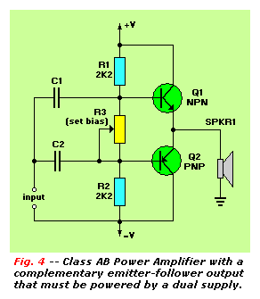
The Class AB amplifier shown in Fig. 4 avoids both transformers and the need to match
transistors. A complementary pair of transistors (Q1 and NPN and Q2 a PNP) is connected as an emitter follower.
Powered by a split (dual) supply, the circuit's two emitter followers are biased through R1 and R2 so that their
outputs are at zero volts; no current flows in the speaker under quiescent conditions.
Nevertheless, a slight forward bias can be applied with trimmer potentiometer R3 so that Q1 and Q2 pass modest
quiescent currents to prevent crossover distortion. Identical input signals are applied through C1 and C2 to the base
of the emitter followers, which avoid a split-phase drive.
When an input signal is applied to the Fig. 4 circuit, the positive swing drives PNP Q2 off while driving NPN Q1 on.
Transistor Q1 acts as current source with a very low output (emitter) impedance if feeds a faithful unity-gain copy
of the input voltage signal to the speaker. The transistor characteristics have little or no effect on this response.
Similarly, negative swings of the input signal drive Q1 off and Q2 on. Because Q2 is a PNP BJT, it becomes a current
sink with minimal input (emitter) impedance. It also produces a faithful unity-gain copy of the voltage signal to
the speaker, again with Q2's characteristics having little or no effect on the circuit's response.
As a result, the Fig. 4 circuit does not require that Q1 be matched to Q2, and neither input nor output transformers
are required.
Modification of this circuit, as shown in Figs. 5-a and b, work from
single ended power supplies. In Fig. 5-a, one side of the speaker is connected to the amplifier through
high-value blocking capacitor C3 and, and the other end is connected to ground; in Fig. 5-b,
one side is connected to C3 and the other side is connected to the positive supply. All three circuits are popular in
modern high-fidelity audio power amplifiers based on integrated circuitry.
Class AB Variations:
The circuit in Figs. 4-a is a unity-voltage gain amplifier so one obvious improvement
is to add a voltage-amplifying driver stage, as shown in Figs. 6. Transistor Q1,
configured as a common-emitter amplifier, drives two emitter followers, Q2 and Q3, through its collector load resistor R1.
Note that Q1's base bias is derived from the circuit's output through resistors R2 and R3. This configuration
provides DC feedback to stabilize the circuit's operating points and AC feedback to minimize signal distortion.
The Fig. 6 circuit illustrates how a form of auto-bias can be applied to Q2 and Q3 through the silicon diodes D1 and
D2. If the simple voltage-divider biasing method in Fig. 4 is used in the Fig. 6 circuit, its quiescent current will
increase as ambient temperature rises and decrease as it fall. (This is caused by the thermal characteristics of a
transistor's base-emitter junction.)
The biasing in Fig. 6 is derived from the forward voltage drop of series diodes D1 and D2 whose thermal characteristics
are closely matched to those of the base-emitter junctions of Q2 and Q3. Consequently, this circuit offers excellent
thermal compensation.
Practical amplifiers include a pre-set trimmer potentiometer in series with D1 and D2. This component makes it
possible to adjust biased voltage over a limited range. Low-value resistors R4 and R5 in series with the emitters of
Q2 and Q3 provide some negative DC feedback.
The impedance of the Fig. 4 circuit equals the product of the speaker load impedance and the current gain of either Q1
or Q2. The circuit can be improved by replacing transistors Q1 and Q2 with Darlingron pairs which will significantly
increase the circuit's input impedance and increase the amplifier's collector load capacity.
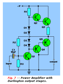
Figures 7 to 9 show three different ways of modifying the Fig. 6 circuit by replacing
individual transistors with Darlington pairs. For example, in Fig. 7, transistors Q2 and Q3 form a Darlingron NPN
pair, and Q4 and Q5 form a darlington PNP pair. There are four base-emitter junctions between the bases of Q2 and Q4,
and the output circuit is biased with a string of four silicon diodes, D1 and D4, in series to compensate for the
Darlingron pairs.
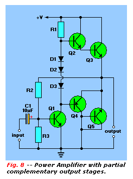
Figure 8, Q2 and Q3 are a Darlington NPN pair, but Q4 and Q5 are a complementary pair of
common-emitter amplifiers. They operate with 100% negative feedback, and provide unity-voltage gain and very high
input impedance. Thisquasi-complementary output stage is probably the most popular Class AB power amplifier
topology today. Notice the three silicon biasing diodes, D1, D2, and D3.
Finally, in Figure 9, both pairs Q2 and Q3 and Q4 and Q5 are complementary pair of
unity-gain, common-emitter amplifiers with 100% negative feedback. Because the pairs produce outputs that are mirror
images of each other, the circuit has a complementary output stage. Notice that this circuit has only two silicon
biasing diodes, D1 and D2.
Amplified Diodes:
The circuits in Figs. 6 to 9 include strings of two to four silicon biasing diodes.
Each of those strings can be replaced by single transistor and two resistors configured as an amplified diode,
as shown in Figs. 10.
The output voltage of the circuit, Vout can be calculated from the formula:
Vout = VBE x R1 + R2/R2
If resistor R1 is replaced by a short circuit, the circuit's output will be equal to the base-emitter junction "diode"
voltage of Q1 (VBE). The circuit will then have the thermal characteristics of a
discrete diode.
If resistor R1 equals R2, the circuit will act like two series-connected diodes, and if R1 equals three times R2, the
circuit will act like four series-connected diodes, and so on. Therefore, the circuit in Figs. 10 can be made to
simulate any desired whole or fractional number of series-connected diodes, depending on how the R1/R2 ratios are
adjusted.
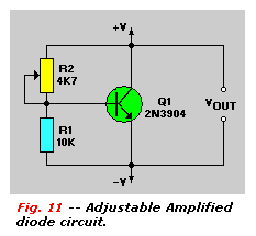
Figure 11 shows how the circuit in Fig. 10 can be modified to act as a fully adjustable
"amplifier diode", with an output variable from 1 to 5.7 times the base-emitter junction voltage
(VBE)
Bootstrapping:
The main purpose of the Q1 driver stage in Fig. 6, the base complementary amplifier, is
to give the amplifier significant voltage gain. At any given value of Q1 collector current, this voltage gain is
directly proportional to the effective Q1 collector load value. It follows that the value of resistor R1 should be
as large as possible to maximize voltage gain. However, there are several reasons why this does not work.
First, the effective or AC value of R1 equals the actual R1 value shunted by the input impedance of the Q2-Q3
power amplifier stage. Therefore, if R1 has a higher value, the power amplifier input impedance must be even greater.
That can usually be done by replacing Q2 and Q3 with high-gain transistor pairs, as was done in Figs. 7 to 9.
The second reason is that Q1 in Fig. 6 must be biased so that its collector assumes a quiescent half-supply voltage
value to provide maximum output signal swings; this condition is set by the Q1's collector current and resistor R1's
value.
The true value of R1 is predetermined by biasing requirements. To achieve high voltage gain, a way must be found to
make the AC impedance of R1 much greater than its DC value. This is accomplished with he bootstrapping technique
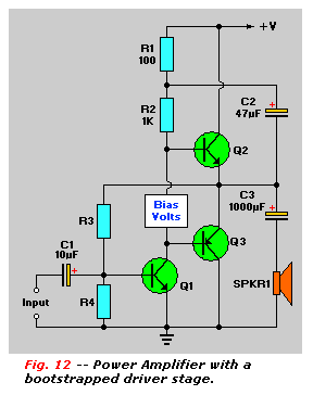
shown in Figs. 12 & 13.
In Fig. 12, Q1's collector load consists of R1 and R2 in series. The circuit's output
signal, which also appears across SPKR1, is fed back to the R1-R2 junction through C2. This output signal is a near
unity-voltage-gain copy of the signal appearing on Q1's collector.
If resistor R1 has a value of 1 kilohm, the Q2-Q3 stage provides a voltage gain of 0.9. As a result, an undefined
signal voltage appears at the low end of resistor R2, and 0.9 times that undefined voltage appears at the top of R2.
In other words, only one-tenth of the unknown signal voltage is developed across R2. Therefore, it passes one-tenth
of the signal current that would be expected from a 1-kilohm resistor.
This means that the AC signal impedance value of R2 is ten times greater (10-kilohms) than its DC value, and the signal
voltage gain is increased correspondingly. In practical circuits, "bootstrapping" permits the effective voltage gain
and collector load impedance of Q1 to be increased by the factor of about twenty.
Fig. 13 is the schematic for an alternative version of Fig. 12 without one resistor and
one capacitor. In this circuit. SPKR1 is part of Q1's collector load, and it is bootstrapped through capacitor C2.
As an alternative to bootstrapping, the load resistor can be replaced with a simple transistor constant-current
generator. This design is found in many integrated circuit audio power amplifiers.
Alternative Drivers:
Returning once again to Fig. 6, notice that parallel DC and AC voltage form the R1-R2 divider network is fed back to
the Q1 driver stage. This is a simple and stable circuit, but its gain and input impedance are low. Moreover, it
will work only over a limited power supply voltage range.
Figure 14 is a variation of the Fig. 6 circuit intended to function as a driver stage.
Current feedback through
resistors R1 and R2 allows the circuit to work over a wide supply voltage range. The feedback resistors can be AC
decoupled (as shown) through C2 to increase the gain and input impedance, but at the expense of increased signal
distortion. Transistor Q1 can be replaced with a Darlington pair if very high input impedance is desired.
Another alternative driver stage, Fig. 15, depends on series DC and AC feedback to give it
more gain and higher input impedance than can be obtained from the Fig. 6 circuit. In this circuit, PNP transistor
Q1 is directly coupled to NPN transistor Q2.
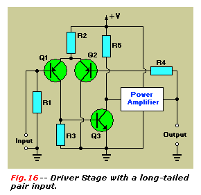
Finally, Fig. 16 is the schematic for a driver circuit specifically intended for use in
amplifiers with dual or split power supplies that have direct-coupled input and output stages referenced to ground.
The input stage of this driver stage is a long-tailed pair. Both the input and output will be centered on DC ground
if the values of resistors R1 and R4 are equal. This circuit is found in many integrated circuit power amplifiers. An IC power amplifier:
Improvements in the power-handling capabilities of monolithic integrated circuits have permitted power amplifier to be
integrated on a single silicon substrate or chip. The techniques for designing integrated circuit power amplifiers
are similar to those for discrete device circuits. It turns out that the similarities between discrete and IC power
amplifier designs are closer than for most other linear circuits.
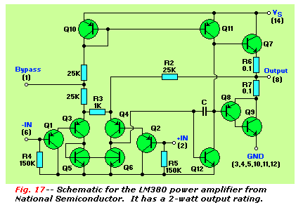
Figure 17 is a simplified circuit diagram for the LM380, an IC power amplifier, drawn in
the manufacturer's data book style. The LM380 was developed by National Semiconductor Corporation for consumer
applications. It features an internally fixed gain of 50 (34 dB) and an output that automatically centers itself at
one-half of the supply voltage.
An unusual input stage permits inputs to be referenced to the ground or AC coupled, as required. The output stage of
the LM380 is protected with both short-circuit current limiting and thermal-shutdown circuitry.
The LM380 has two input terminals. Both Q1 and Q2 are connected as PNP emitter followers that drive the Q3 and Q4
differential amplifier transistor pairs. The PNP inputs reference the input to gro8und, thus permitting direct
coupling of the input transducer.
The output is biased to half the supply voltage by resistor ratio R1/R2 (resistor R1 is formed by two 25-kilohm
resistors and R2 has a value of 25-kilohms). Negative DC feedback, through resistor R2, balances the differential
stage with the output at half supply, because R1 = R2.
The output of the differential amplifier stage is direct coupled into the base of Q12, which is a common-emitter,
voltage-gain amplifier with a constant current-source load provide by Q11. Internal compensation is provided by the
pole-splitting capacitor C'. Pole-splitting compensation permits wide power bandwidth (100 KHz at 2 watts, 8 ohms).
The collector signal of Q12 is fed to output pin 8 of the IC through the combination of emitter-coupled Q7 and the
quasi-complementary pair emitter followers Q8 and Q9. The short-circuit current is typical 1.3 amperes.
 The Class A circuit amplifies audio output with minimum distortion, but transistor Q1 consumes current
continuously--even in the quiescent state--giving it low efficiency. Amplifier efficiency is defined as the
ratio of AC power input to the load divided by the DC power consumed by the circuit.
The Class A circuit amplifies audio output with minimum distortion, but transistor Q1 consumes current
continuously--even in the quiescent state--giving it low efficiency. Amplifier efficiency is defined as the
ratio of AC power input to the load divided by the DC power consumed by the circuit.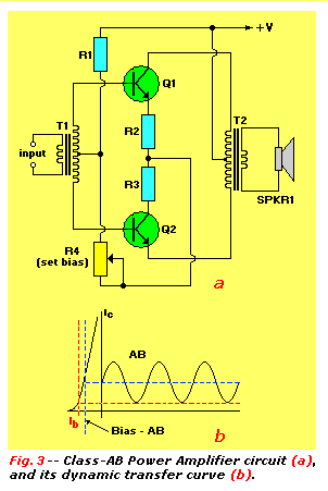
 Nevertheless, a slight forward bias can be applied with trimmer potentiometer R3 so that Q1 and Q2 pass modest
quiescent currents to prevent crossover distortion. Identical input signals are applied through C1 and C2 to the base
of the emitter followers, which avoid a split-phase drive.
Nevertheless, a slight forward bias can be applied with trimmer potentiometer R3 so that Q1 and Q2 pass modest
quiescent currents to prevent crossover distortion. Identical input signals are applied through C1 and C2 to the base
of the emitter followers, which avoid a split-phase drive.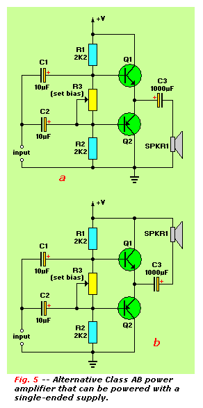 Modification of this circuit, as shown in Figs. 5-a and b, work from
single ended power supplies. In Fig. 5-a, one side of the speaker is connected to the amplifier through
high-value blocking capacitor C3 and, and the other end is connected to ground; in Fig. 5-b,
one side is connected to C3 and the other side is connected to the positive supply. All three circuits are popular in
modern high-fidelity audio power amplifiers based on integrated circuitry.
Modification of this circuit, as shown in Figs. 5-a and b, work from
single ended power supplies. In Fig. 5-a, one side of the speaker is connected to the amplifier through
high-value blocking capacitor C3 and, and the other end is connected to ground; in Fig. 5-b,
one side is connected to C3 and the other side is connected to the positive supply. All three circuits are popular in
modern high-fidelity audio power amplifiers based on integrated circuitry.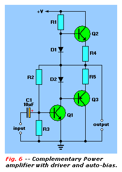 The impedance of the Fig. 4 circuit equals the product of the speaker load impedance and the current gain of either Q1
or Q2. The circuit can be improved by replacing transistors Q1 and Q2 with Darlingron pairs which will significantly
increase the circuit's input impedance and increase the amplifier's collector load capacity.
The impedance of the Fig. 4 circuit equals the product of the speaker load impedance and the current gain of either Q1
or Q2. The circuit can be improved by replacing transistors Q1 and Q2 with Darlingron pairs which will significantly
increase the circuit's input impedance and increase the amplifier's collector load capacity.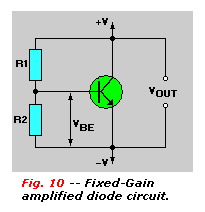
 The second reason is that Q1 in Fig. 6 must be biased so that its collector assumes a quiescent half-supply voltage
value to provide maximum output signal swings; this condition is set by the Q1's collector current and resistor R1's
value.
The second reason is that Q1 in Fig. 6 must be biased so that its collector assumes a quiescent half-supply voltage
value to provide maximum output signal swings; this condition is set by the Q1's collector current and resistor R1's
value.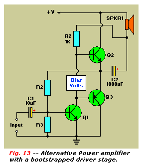 Alternative Drivers:
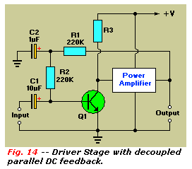 Figure 14 is a variation of the Fig. 6 circuit intended to function as a driver stage.
Current feedback through
resistors R1 and R2 allows the circuit to work over a wide supply voltage range. The feedback resistors can be AC
decoupled (as shown) through C2 to increase the gain and input impedance, but at the expense of increased signal
distortion. Transistor Q1 can be replaced with a Darlington pair if very high input impedance is desired.
Figure 14 is a variation of the Fig. 6 circuit intended to function as a driver stage.
Current feedback through
resistors R1 and R2 allows the circuit to work over a wide supply voltage range. The feedback resistors can be AC
decoupled (as shown) through C2 to increase the gain and input impedance, but at the expense of increased signal
distortion. Transistor Q1 can be replaced with a Darlington pair if very high input impedance is desired.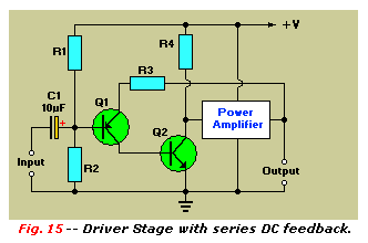
 An IC power amplifier: