Despite these advantages, the FET has not replace the bipolar transistor in all applications, but it has encouraged new generations of small-signal and general purpose and RF MOSFET's as well as general purpose and RF MOSFET power transistors.
Moreover, the latest digital logic families are based on FET technologies. The basic FET is a simple, three-terminal, voltage-controlled device with characteristics that are similar to those of vacuum-tube pentodes. Thus, the FET is considered to be the solid-state equivalent of a pentode.
The two major classes of FET's are the Junction FET (JFET) and Metal-Oxide-Semiconductor FET (MOSFET), formerly called an insulated-gate-FET (IGFET). FET's are further divided into N-channel, P-channel, depletion-mode, and enhancement-mode devices. MOSFET's with N-doped channels are called NMOS, and those with P-doped channels are referred to as PMOS.
The three electrodes in all FET's are the source, drain and gate, analogous to the emitter, collector, and base of the bipolar transistor. Both JFET's and MOSFET's are available as discrete transistors. Some MOSFET's have dual gates and are intended for use as radio-frequency mixers.
This article explains how P-channel adn N-channel MOSTFET's are combined to form the popular complementary-MOS (CMOS) digital logic families. CMOS technology has made possible very large scale integrated (VLSI) memories, microprocessors and dedicated circuits that contain more than one million transistors and still have very low power requirements.
Most small-signal FET's today are fabricated with planar geometry in which all electrodes are accessible from the top of the device. The active regions are defined on the wafer or substrate by successive masking, etching, and deposition or ion-implantation steps. But power MOSFET' now being fabricated with vertical structures are actually capable of handling much higher current in smaller areas of silicon.
 Junction FET's:
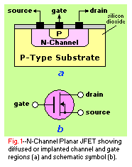
The simplest FET, the JFET, is illustrated by the cross-section view of Fig. 1-a. It is made by selectively implanting or diffusing ions into the wafer or substrate. An N-type region is defined on the P-type substrate by photolithographic methods, and N-type ions are implanted to form the N-channel. Later in the manufacturing process, following further masking, oxide-deposition and etching steps, P-type ions are implanted or diffused into the N-channel to form the P-type gate.
Aluminum source and drain terminal are formed directly on the N-channel and an aluminum gate terminal is formed to the P-type gate. The symmetrical construction of the JFET permits the drain adn source to be interchanged, if necessary.
If a positive voltage is applied at the drain of the N-channel JFET shown in Fig. 1-a, and a negative voltage is applied at the source with the gate terminal open, a drain current flows. When the gate is biased negative with respect to the source, the PN junction is reverse biased, and a depletion region, devoid of current carriers, is formed.
Because the N-channel is more lightly doped than the P-type gate material, the depletion region penetrates into the N-channel. This region, depleted of charge carriers, behaves like an insulator. The depletion region narrows the N-channel and increases its resistance. If the bias is made even more negative, drain current is cut off completely.
The gate-bias voltage that cuts off the drain current is called the pinchoff or gate-cut-off voltage. However, as the bias becomes positive, the depletion region recedes, the channel resistance is reduced, and drain current increases. Thus, the JFET gate actually controls JFET current.
 The schematic symbol for the N-channel JFET is shown in Fig. 1-b. As in other schematic
symbols for solid-state devices, the arrowhead (representing the direction of conventional current flow) points form
P-doped material to N-doped material. In the N-channel JFET symbol, the arrowhead points from the P-type gate toward
the N-type channel.
The schematic symbol for the N-channel JFET is shown in Fig. 1-b. As in other schematic
symbols for solid-state devices, the arrowhead (representing the direction of conventional current flow) points form
P-doped material to N-doped material. In the N-channel JFET symbol, the arrowhead points from the P-type gate toward
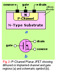
the N-type channel.A section view of a P-channel JFET is shown in Fig. 2-a. The channel of the device is P-type material, and the gate is N-type. If a positive voltage is applied to the source, conventional current flows from the source to the drain. To reverse bias the junction between the N-type gate and the P-type channel, the gate must be made positive with respect to the channel. The biasing voltages of a P-channel JFET are opposite to those of the N-channel JFET>
The schematic symbol for the P-channel JFET is shown in Fig. 2-b. The arrowhead also points form P-type material to N-type material. In this instance, it points from the P-type channel to the N-type gate region. The characteristics of the P-channel JFET are similar to those of the N-channel device, except that the voltage and current polarities are reversed.
 Both N-type and P-type JFET's operate in the depletion mode; that is, they conduct with zero bias on their gates.
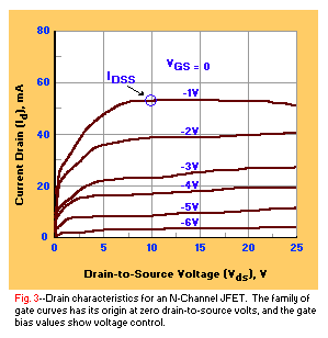
Figure 3 shows a typical family of drain characteristics for an N-channel JFET. As
the gate-to-source voltage is made increasingly negative, the depletion region is increased, and drain current
decreases. As a result, pinchoff voltage occurs at a lower value of VDS. Curves for
different values of gate-to-source bias, VGS, are plotted in the figure because the
FET is a voltage-operated device.
Both N-type and P-type JFET's operate in the depletion mode; that is, they conduct with zero bias on their gates.
Figure 3 shows a typical family of drain characteristics for an N-channel JFET. As
the gate-to-source voltage is made increasingly negative, the depletion region is increased, and drain current
decreases. As a result, pinchoff voltage occurs at a lower value of VDS. Curves for
different values of gate-to-source bias, VGS, are plotted in the figure because the
FET is a voltage-operated device.JFET Circuits:
When an N-channel JFET is connected to a VDS supply as shown in Fig. 4, a drain current, ID can be controlled by a gate-to-source bias voltage, VDS. Similarly, when a P-channel JFET is connected to a negative drain voltage, a drain current, ID, flows in the device. The value of ID is maximum when VGS equals zero, and it is reduced (to bring the JFET into a linear operating region) by applying a reverse bias to the gate terminal of the device (negative bias in a N-channel devices, positive bias in a P-type).
In Fig. 3, the value of VGS to reduce ID to zero, the gate-to-source pinchoff voltage VP is about -7 volts. The value of ID when VGS equals zero (called IDSS or saturation current for zero bias) is about 52 milli-amperes for the device shown in the figure.
The gate-to-source junction of the JFET has the characteristics of a silicon diode. When reverse biases (to bring it into its linear operating region), gate leakage currents (IGSS) are measured in thousandths of a micro-ampere at room temperature. Actual gate signal currents are only a fr4action of that, and the input impedance to the gate is typically 1000 megohms at low frequencies. The gate junction is effectively shunted by a capacitance of a few picofarads, so input impedance falls as input frequency is increased.
If the gate-to-source junction of the JFET is forward biased, it conducts like a normal silicon diode, and if it is severely reverse biased it avalanches like a Zener diode. Neither of those conditions will harm a JFET if its gate currents are limited to those specified.
 Referring to the N-channel JFET drain characteristics in Fig. 3, it can be seen that, for each value of
VGS, drain current ID rises linearly from zero as
the drain-to-source voltage (VDS) is increases from zero to a value at which a
knee occurs on each curve. Moreover, ID remains virtually constant as
VDS is increased beyond where the knee occurs.
Referring to the N-channel JFET drain characteristics in Fig. 3, it can be seen that, for each value of
VGS, drain current ID rises linearly from zero as
the drain-to-source voltage (VDS) is increases from zero to a value at which a
knee occurs on each curve. Moreover, ID remains virtually constant as
VDS is increased beyond where the knee occurs.Thus, when VDS for any of the family of VGS curves is below its knee value, the drain-to-source pins of the JFET act like a voltage-variable resistor with value determined by VGS. The drain-to-source resistance, RDS, can be varied from several hundred ohms at VGS = zero to thousands of megohms at pinchoff. That characteristic permits the JFET to be used in a circuit as a voltage-controlled switch.
From the drain characteristic curve of Fig. 3, it can be seen that when VDS is above the knee value, the ID value is dictated primarily by the VGS value, and is virtually independent of the VDS value. This characteristic permits the JFET to function as a voltage-controlled current generator.
The gain of a JFET is specified as a transconductance, gm, the rate of change of drain current with respect to gate voltage. A gm of 5 milli-amperes per volt indicates that a variation of one volt on the gate produces a change of 5 milli-amperes ID. The units of this measurement are in inverse ohms or mhos. You will find that JFET data sheets usually specify gm in millimhos or micromhos.
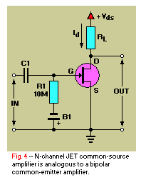
The N-channel JFET in Fig. 4 is organized as a common-source amplifier, analogous to a bipolar NPN common-emitter amplifier. In typical applications, the JFET is biased into its linear region and organized as a voltage-to-voltage converter or amplifier. As shown in Fig. 4, a load resistor of suitable value, RL, should be placed in series with the JFET's drain-to-source current.
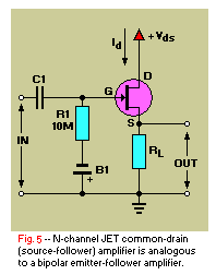
 Another common JFET configuration is the common drain or source-follower configuration shown in
Fig. 5. That configuration is analogous to the bipolar emitter-follower configuration.
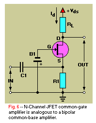
Yet another possible JFET configuration is the common-gate configuration shown in Figure 6.
That configuration is analogous to a bipolar common-base configuration.
Another common JFET configuration is the common drain or source-follower configuration shown in
Fig. 5. That configuration is analogous to the bipolar emitter-follower configuration.
Yet another possible JFET configuration is the common-gate configuration shown in Figure 6.
That configuration is analogous to a bipolar common-base configuration.MOSFET's Explained:
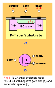
The metal-oxide-FET or MOSFET was developed as an improvement on the JFET, and it has become the most important form of FET. Figure 7-a illustrates an N-channel depletion-mode MOSFET with a negative gate bias. The gate of this MOSFET is fully insulated from the adjacent channel. This is the most important distinction between an N-type depletion-mode MOSFET and an N-type JFET, which is manufactured with a doped gate region directly under and in contact with the gate.
The surface of the silicon P-type wafer is first coated with a layer of silicon dioxide (SiO2), and the source and drain windows are masked and etched to expose the P-type substrate. N-dopants are heavily diffused or implanted into those regions. Another window is masked and etched over the channel, and it is given a lighter concentration of N dopant. In subsequent steps, the channel is recoated with an insulating oxide, and the metal source, drain, and gate terminals are deposited.
When the drain is positive with respect to the source, a drain current will flow, even with zero gate voltage. However, if the gate is made negative with respect to the substrate, positive charge carriers (holes) induced in the N-channel will combine with the electrons and cause channel resistance to increase. With increasing negative bias, the pinchoff voltage will be reached, and drain current will cease. However, if the gate is made positive with respect to the substrate, additional electrons are induced, and the channel current then increases.
The schematic symbol for the N-type depletion-mode MOSFET is shown in Figure 7-b. The path or channel between the source and drain is shown as a solid bar. THe symbol for the P-channel depletion-mode MOSFET is identical to the N-type, except that the arrow points outwards.
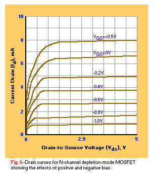
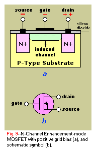 Figure 8 is a drain-to-source characteristic curve for an N-channel depletion-mode MOSFET.
It can be seen that the current drain, ID, is inversely proportional to the magnitude
of the negative gate voltages, VGS. Compare Fig. 8 with Fig. 3 for the N-channel JFET
to see their similarities.
Figure 8 is a drain-to-source characteristic curve for an N-channel depletion-mode MOSFET.
It can be seen that the current drain, ID, is inversely proportional to the magnitude
of the negative gate voltages, VGS. Compare Fig. 8 with Fig. 3 for the N-channel JFET
to see their similarities.Planar enhancement-mode MOSFET's are made by the same methods as planar depletion-mode MOSFET's. However, the N-channel enhancement-mode MOSFET shown in Fig. 9 does not have the N-doped drain-to-source channel through the P-type substrate of the N-channel depletion-mode MOSFET. Therefore, there is no conduction between drain and source at zero gate bias.
 To turn an enhancement-mode MOSFET on, positive gate bias is needed. As the gate voltage is increased, more electrons
are induced into the channel. They cannot flow across the oxide layer of the gate, so they accumulate at the substrate
surface below the gate oxide.
To turn an enhancement-mode MOSFET on, positive gate bias is needed. As the gate voltage is increased, more electrons
are induced into the channel. They cannot flow across the oxide layer of the gate, so they accumulate at the substrate
surface below the gate oxide.When a sufficient number of electrons has accumulated, the P-type substrate material is converted into an N-channel, and drain-to-source conduction occurs. The magnitude of the drain current depends on the channel resistance, but it is controlled by the gate voltage.
The schematic symbol for an N-type enhancement-mode MOSFET is shown in Fig. 9-b. In this symbol, the gate does not make direct contact with the channel. The arrowhead points from the P-type substrate toward the (induced) N-type channel, shown as a line broken into three sections to indicate an intermittent current channel.
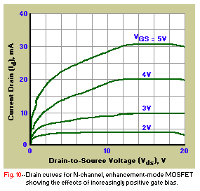
Current flow in the channels of both kinds of enhancement-mode MOSFET's is proportional to the voltage on their gates, VGS. this can be seen for an N-type enhancement-mode MOSFET by examining the family of gate voltage VGS curves in Fig. 10. Current drain, ID, is directly proportional to the positive value of gate voltage.
A P-channel enhancement-mode MOSFET is made the same way as the N-channel device except that P-channel drain and source regions are diffused into an N-type substrate. The symbol for a P-type enhancement-mode MOSFET is the same as the one shown in Fig. 9-b except that the direction of the arrow is reversed. In the case of a P-type enhancement-mode MOSFET, the drain current is directly proportional to the negative values of its grid voltage.
The high gate impedance of all MOSFET's, makes them susceptible to damage from even low-energy electrostatic discharge (ESD). For this reason many discrete MOSFET's and IC's based on MOSFET's are protected with on-chip Zener diode circuits.
CMOS Logic Devices:
An enhancement-mode MOSFET can act as a switch when it is turned on or off by a voltage applied to the gate electrode: N-channel MOSFET's are switched with positive gate voltage, and P-channel MOSFET's are switched with negative voltage. These are known as complementary responses, and they form the basis for complementary MOS or CMOS digital logic families.
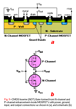 Figure 11-a is a section view of a complementary pair of MOSFET's on a common substrate,
the basic topography for all CMOS gates. The common substrate that is used for this pair is an N-doped silicon wafer.
To make an N-channel MOSFET on an N-doped substrate, it is necessary to diffuse or implant a P-doped well in the
substrate. The smaller N-type wells can then be formed in this P-doped region.
Figure 11-a is a section view of a complementary pair of MOSFET's on a common substrate,
the basic topography for all CMOS gates. The common substrate that is used for this pair is an N-doped silicon wafer.
To make an N-channel MOSFET on an N-doped substrate, it is necessary to diffuse or implant a P-doped well in the
substrate. The smaller N-type wells can then be formed in this P-doped region.Because the substrate is N-doped, fewer steps are required to form the P-channel FET. The P- and N-doped guard bands isolate and insulate the individual transistors in this integrated circuit to prevent mutual interference. Although not illustrated here, these guard bands are actually N- or P-doped rings formed around the complete FET below the oxide layer in this CMOS technology.
The two transistors in the section view, Fig. 11-a, can be connected to form a CMOS logic inverter, the simplest of digital logic circuits. This is accomplished by connecting the gates together to form an input (VIN) terminal, and taking the output (VOUT) from the common drain. The source on the left side of the diagram, VSS, is grounded, while the source on the right side is connected to the positive supply, VDD.
Those connections are schematically shown in Figure 11-b. How does the inverter work? Consider the P-channel device to be the driver and the N-channel device to be the load. Recall that an N-channel enhancement MOSFET conducts with a negative gate voltage.
When the voltage input to the inverter is low (logic 0), the gate voltage of the P-channel device is negative, equal to the supply voltage VDD. As a result, the P-channel MOSFET is switched on, and there is a low impedance path from the output to VDD. Because the N-channel is off (gate voltage is zero), there is a very high impedance path from the output to ground. Therefore, the output voltage rises to VDD.
When the input voltage is high (logic 1), the situation is reversed. The P-channel FET is cut off, and the N-channel FET is on, so the output voltage falls to zero. Therefore, the circuit is a logic inverter: a low input results in a high output, and vice versa.
In either logic state one FET is ON while the other is OFF. Because one FET is always turned OFF, the quiescent current of the the CMOS unit is extremely low. These properties of N- and P-type enhancement-mode FET's combined to form CMOS gates provide many advantages:
- Extremely low power consumption.
- Wide power supply voltage range.
- High DC noise margin.
- High input impedance.
- Wide operating temperature range.
Power MOSFET's:
Power MOSFET's exhibit the properties of small-signal MOSFET's such as high-input impedance and voltage control, and they have drains, sources and gater, but they are designed to handle higher currents. As majority-carrier devices that store no charges, they can switch faster than bipolar power transistors.
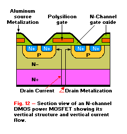
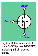 Figure 12 is a section view of an N-Channel, enhancement-mode power MOSFET. Unlike its
small-signal counterpart, the latest power MOSFET's are fabricated with vertical rather than planar structures. They
are made with the double diffused (DMOS) process, and they have conductive silicon (polysilicon) gates. The gate of
this device is isolated from the source by a layer of insulating silicon oxide.
Figure 12 is a section view of an N-Channel, enhancement-mode power MOSFET. Unlike its
small-signal counterpart, the latest power MOSFET's are fabricated with vertical rather than planar structures. They
are made with the double diffused (DMOS) process, and they have conductive silicon (polysilicon) gates. The gate of
this device is isolated from the source by a layer of insulating silicon oxide.When a voltage is applied between the gate and source terminals, an electric field is set up within the MOSFET. This field alters the resistance between the drain and source terminals, and it permits conventional current to flow in the drain in response to the applied drain circuit voltage. There are also P-channel, enhancement-mode power MOSFET's in which conventional current flows in the opposite direction of the N-channel device. Fig. 13 is the schematic symbol for a DMOS enhancement-mode, N-channel power MOSFET.
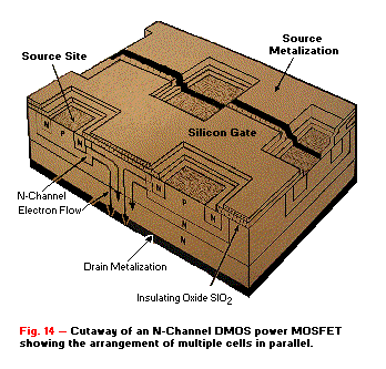
Figure 14 is an cutaway view of a typical DMOS power MOSFET. It is made up of many cells or transistor element connected in parallel. Each source cell consists of a closed rectangular or hexagonal channel which separates a source region from the substrate drain body. The cells are formed in an integrated circuit process, and there might be more than a half million cells per square inch of substrate. All of the source cells are connected in paralleled by a continuous deposition of aluminum metallization, which forms the grid-like common source terminal.
 The DMOS power MOSFET contains an inherent PN junction diode, and its equivalent circuit can be considered as a diode
in parallel with the source-to-drain channel, as shown in the schematic symbol of Fig. 13.
The DMOS power MOSFET contains an inherent PN junction diode, and its equivalent circuit can be considered as a diode
in parallel with the source-to-drain channel, as shown in the schematic symbol of Fig. 13.International Rectifier (IR) makes DMOS power MOSFET's that have hexagonally shaped cells, so it calls its products HEXFET's. Motorola Semiconductor also offers DMOS products MOSFET's, but its devices have rectangular rather than hexagonal cells. Motorola named its power MOSFET's TMOS to call attention to the T-shaped current flow that occurs in the cells between the common drain and the channels to the multiple sources.
Power MOSFET's are widely specified for high-frequency switching power supplies (generally those that switch at frequencies above 100kHz), AC and DC motor speed controls, high-frequency generators for induction heating, ultrasonic generators, audio amplifiers, and amplitude modulation transmitters.
The advantages to using power MOSFET's over power bipolar transistors include:
- Faster switching speeds and lower switching losses.
- Absence of the bipolar's second breakdown.
- Wider safe operating area.
- Higher input impedance.
- High, if not higher, gain.
- Faster rise and fall times.
- Simple drive circuitry.
Radio-Frequency power MOSFET's are now available that will operate over the 2 to 200 MHz frequency range. The high power and high gain of these devices makes them suitable as power amplifiers in solid-state transmitters for FM and TV br5oadcasting.
Copyright and Credits:
© 1993 Original author Ray Marston. Electronics Now, March 1993. Published by Gernsback Publishing. (Gernsback Publishing is (sadly) out of business since January 2000).
All graphics, drawings, photos, © 2006 Tony van Roon.
Re-posting or taking graphics in any way or form from this website or of this project is expressly prohibited by international copyright laws. Permission by written consent only.
Continue with Transistor Tutorial Part 10: "MOSFet's"
Copyright © 2006 - Tony van Roon, VA3AVR
Last updated: December 18, 2009