Home » Circuits
Handy Time Delay With Relay Output
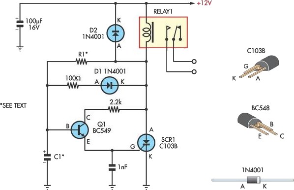
This circuit is designed to provide delayed relay switching action at power on. The delay is a function of the time constant produced by the combination of R1 and C1. At power on, C1 charges slowly via R1 and the coil of the relay. When the voltage across C1 exceeds both the base-emitter voltage of Q1 and the gate trigger voltage of the SCR, gate current flows. This fires the SCR and switches on the relay. At power off, diode D1 rapidly discharges C1 through the 100O resistor, so ensuring that every time the circuit is restarted, as in a temporary outage, the delay time is maintained.Circuit diagram:
Just about any NPN transistor can be used for Q1, since after SCR1 fires, it is effectively out of the circuit. In fact, the only part that’s still active after SCR1 turns on is the relay. You can’t get much simpler than that! This circuit can be used to delay speaker turn-on, so avoiding the "thump" that occurs in some stereo systems at power on. A 5-second delay is enough for this application, requiring approximately 560kO for R1 and 10µF for C1. Another application might be as a motor protector in a short power outage.
Author: R. Besana - Copyright: Silicon Chip Electronics

