Home » Circuits
High Input Voltage Linear Regulator
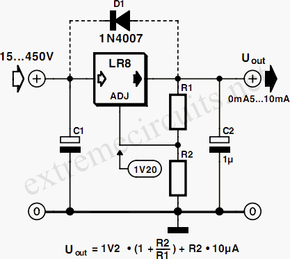
Commonly used 3-pin linear voltage regulators, for example the LM317, cannot handle input voltages in excess of about 30V. The LR8A from Supertex Inc is a new, adjustable three pin regulator that can accept input voltages up to 450V and can supply an output current of 0.5mA to 10mA. Using this device it is possible to work with rectified 230VAC. The LR8 has a wide input voltage range of +12 V to +450V. Two external resistors (R1 and R2) allow the output voltage to be adjusted from 1.20 V to 440 V provided that the input voltage is at least 10 V greater than the output voltage. The LR8 adjusts the voltage difference between the Vout and ADJ pins to a nominal value of 1.20V.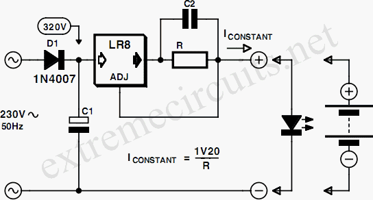 This 1.20V is amplified by the external resistor ratio of R1 and R2. An internal constant bias current of 10µA is connected to the ADJ pin so that Vout is increased by a constant voltage of 10µA times R2. The formula for calculating the output voltage is given next to the circuit diagram. To ensure stable operation of the regulator a minimum output current of 500µA is necessary and a bypass capacitor of minimum 1.0µF should be used. Protection circuits in the LR8 limit the output current to 15mA typically and temperature protection ensures that the device temperature will not exceed 125oC.
 When the device reaches its temperature limit, the output voltage/current will decrease to keep the junction temperature within limits. The two circuit diagrams show the LR8 used as a voltage regulator and as a constant current source. The current source can be used to a drive an LED. This configuration would give an LED with super-wide input voltage range, i.e., from +12V to +450V. The LR8 was originally designed to be used for switch mode supply start-up applications so it incorporates a feature which shuts down the LR8 when the output voltage exceeds the input voltage. Diode D1 is therefore necessary in the voltage regulator circuit diagram to prevent the output voltage exceeding the input voltage at any time.
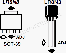 The minimum value of the input capacitor C1 can be calculated from the following formula: C1(min) = (IL t ) / (Vpk – Vout – 10V) Where IL is the load current, and t the period between two voltage peaks. At 50 Hz, using one rectifying diode this will give a value t = 20 ms. Vpk is the peak input voltage, while Vout is the selected output voltage. The LR8 is available in two package outlines. The LR8N8 is a SOT89 SMD package while the LR8N3 is the familiar TO92 Transistor outline (e.g. BC 238). The TO-92 package can dissipate a maximum of 0.74W while with suitable heatsinking, the SMD package can dissipate 1.6W.