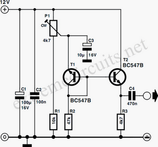
Optimised Semiconductor Noise Source
We have already published designs that use a transistor junction operating in Zener breakdown as a noise source. Anyone who has experimented with a reverse-biased transistor knows that the amplitude of the noise voltage generated in this manner is strongly dependent on the supply voltage. The variation between individual transistors is also rather large. An obvious solution is to use an adjustable supply voltage for the noise generator stage. A BC547B starts to break down at around 8V.

Using P1 and R1, you can adjust the voltage across T1 and R2 between 8 and 12V. C3 decouples the reduced supply voltage. An impedance buffer in the form of T2 and R3 is added to the circuit, to prevent the connected load from affecting the noise source. This buffer is powered directly from the 12-V supply. To adjust this circuit, connect the output to an oscilloscope. Then adjust P1 to obtain the highest signal amplitude, combined with the best ‘shape’ of the noise signal. The output voltage is approximately 300mVpp, and the current consumption is around 2mA.

