Home » Circuits
PWM Modulator
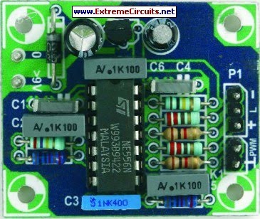
If you ever thought of experimenting with pulse-width modulation, this circuit should get you started nicely. We’ve kept simplicity in mind and used a dual 555 timer, making the circuit a piece of cake. We have even designed a small PCB for this, so building it shouldn’t be a problem at all. This certainly isn’t an original circuit, and is here mainly as an addition to the ‘Dimmer with MOSFET’ article elsewhere in this website. The design has therefore been tailored to this use. A frequency of 500 Hz was chosen, splitting each half-period of the dimmer into five (a low frequency generates less interference).Picture of the project:
 The first timer is configured as a standard astable frequency generator. There is no need to explain its operation here, since this can easily be found on the Internet in the datasheet and application notes. All we need to mention is that the frequency equals 1.49 / ((R1+2R2) × C1) [Hz] R2 has been kept small so that the frequency can be varied easily by adjusting the values of R1 and/or C1. The second timer works as a monostable multivibrator and is triggered by the differentiator constructed using R3 and C3.
Parts layout:
 The trigger input reacts to a rising edge. A low level at the trigger input forces the output of the timer low. R3 and C3 have therefore been added, to make the control range as large as possible. The pulse-width of the monostable timer is given by 1.1xR4xC4 and in this case equals just over a millisecond. This is roughly half the period of IC1a. The pulse-width is varied using P1 to change the voltage on the CNTR input. This changes the voltage to the internal comparators of the timer and hence varies the time required to charge up C4.
Circuit diagram:
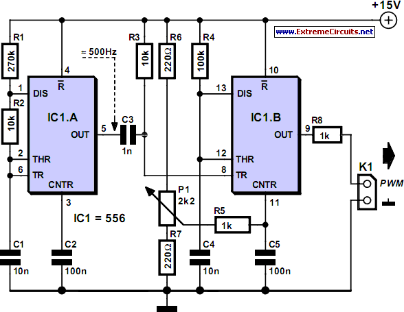 The control range is also affected by the supply voltage; hence we’ve chosen 15V for this. The voltage range of P1 is limited by R6, R7 and R5. In this design the control voltage varies between 3.32 V and 12.55 V (the supply voltage of the prototype was 14.8 V). Only when the voltage reaches 3.51 V does the output become active, with a duty-cycle of 13.5 %. The advantage of this initial ‘quiet’ range is that the lamp will be off. R8 protects the output against short circuits. With the opto-coupler of the dimmer as load, the maximum current consumption of the circuit is about 30 mA.
Power supply:
 COMPONENTS LIST
Resistors:
R1 = 270k
R2,R3 = 10k
R4 = 100k
R5,R8 = 1k
R6,R7 = 220R
P1 = 2k2, linear, mono
Capacitors:
C1,C4 = 10nF
C2,C5,C6 = 100nF
C3 = 1nF
C7 = 2µF2 63V radial
C8 = 100µF 25V radial
Semiconductors:
D1 = 1N4002
IC1 = NE556
IC2 = 78L15
Miscellaneous:
P1 = 3-way pinheader
K1 = 2-way pinheader
Author: Ton Giesberts
Copyright: Elektor Electronics
Copyright: Elektor Electronics