Home » Circuits
Reset Sequencer
It is often necessary in complex designs to provide a sequence of reset pulses to different parts of a circuit to ensure the whole design functions reliably. The DS1830 from Maxim (www.maxim-ic.com) provides three sequenced open-drain reset outputs. This chip is designed for 5 V systems but a 3.3 V version (DS1830A) is also available. Both are offered in a range of package outlines including DIP, SO and µSOP. Two inputs give the chip some degree of programmability of its characteristics: The TOL input defines the chips tolerance to power supply fluctuations before a reset sequence is triggered.Circuit diagram:
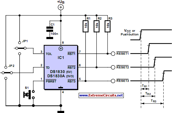
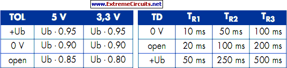 Jumper JP1 allows the TOL to be connected to Ub (Vcc), ground or left open circuit and will result in the following three reset thresholds: The TD input allows the length of the reset signal to be programmed and jumper JP2 gives the following three possibilities: The PBRST (pushbutton reset) allows a manual reset button to be connected to the chip. This input has a built-in 40 k? pull up resistor and can also be driven by a digital output or used to cascade additional devices to provide more sequenced reset signals.
Author: Gregor Kleine
Copyright: Elektor Electronics
Copyright: Elektor Electronics