Home » Circuits
RS232 Voltage Regulator
There are many small applications where it would be preferable to power a device directly from an RS232 (V.24) interface, avoiding a mains power supply. Most ICs require 5 V, and the interface can provide a current of around 8 mA, almost all of which would be consumed by a readily-available voltage regulator, leaving nothing for the actual circuit. Using just four transistors we can construct a voltage regulator with current limiting which will allow us to draw more than the permitted 8 mA from an RS232 interface without damaging it. The example circuit in is configured for an output voltage of 5 V from an input voltage of at least 8 V, and a short-circuit current of 19 mA.The current drawn by the regulator itself is only 0.2 mA. The circuit appears very simple, but it is more cunning than it looks. Few people appreciate what a handy device the transistor is. To meet the requirements for the circuit, the gains of the transistors need to be controlled carefully. Here only B-class devices are used, which have a gain of between about 220 and 280. Diodes D1 to D3 extract the positive voltage from the serial interface. Current limiting is achieved via resistor R1 and transistor T1. As soon as the voltage across the resistor reaches 0.7 V (at 18 mA with R1 = 39 Ω) the transistor turns on and thus turns off the output voltage by turning off T2. The output voltage of 5 V is set by Zener diode D4.
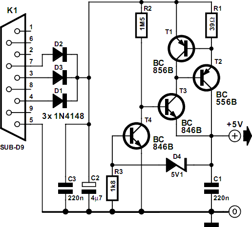
Note that the output voltage is only approximate: beware when using components which have narrow supply voltage tolerances. When the Zener diode voltage and the voltage across transistor T4 are added together, the total is 5.8 V. However, because of T3, the diode is operating at a low current and the actual threshold for T4 is 4.9 V. The main regulation loop is built around R2 and T2. The high value of R2 (1.5 MΩ) is important, since this limits the maximum current through T2. At the output we would like to be able to draw a maximum current of 19 mA. The base of T2 must therefore be supplied with exactly 1/220 (the gain of the transistor) of 19 mA, and likewise the current into the base of T3 should be just 1/220 of 80 µA. With an input voltage of 9 V the voltage drop across R2 will be 3.3V, and so a current of 2.2 µA will flow. Transistor T3 multiplies this current by 220 to 0.5 mA, which is also the minimum quiescent current of the circuit.
Author: M. Müller
Copyright: Elektor Electronics
Copyright: Elektor Electronics