Home » Circuits
Smart Foot Switch
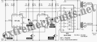
Such jobs as jewel cutting and polishing require the workers to switch on/off two electrical appliances one after another repeatedly for two different services on the same workpiece. This is cumbersome as they need to fully concentrate on delicate handwork on precious jewels. Switching in such situations cannot be done by hand, and doing it by foot using ordinary switches is too tedious. This is mainly because of the difficulty in sensing and controlling the switch position by foot. Ordinary pushbutton switches make or break a contact momentarily, and they can not hold the keypress status. You need a bistable multivibrator with two independent trigger inputs to solve this problem. Here’s a smart foot switch based on dual negative-edge triggered master slave JK flip-flop IC 74LS76 (IC1).J1 and J2 inputs are conneted to 5V through resistors R2 and R5 (each 10k), respectively. K1 and K2 inputs are grounded. Preset pins 2 and 7 are shorted and connected to 5V via resistor R7 (10k). Push-to-on switch S3 connected to the preset inputs is also grounded. Clock and clear inputs of the two flip-flops are cross-connected, i.e. CLK1 (pin 1) is conneted to CLR2 (pin 8) and CLR1 (pin 3) is connected to CLK2 (pin 6). Clock input pins 1 and 6 are pulled up high through resistors R1 and R4 (each 4.7k), respectively. Push-to-on switches S1 and S2 are connected between clock and ground of the flip-flops. Switch S1 activates device 1, while switch S2 activates device 2. Switch S3 activates both device 1 and device 2 simultaneously.
 Device status is indicated by LED1 and LED2. Glowing of LED1 and LED2 indicates that device 1 and device 2, respectively, are in on condition. The LEDs are connected from +5V to Q1 (pin 14) and Q2 (pin 10) of IC1 through resistors R3 and R6, respectively. Initially when the power supply is switched on, Q1 and Q2 outputs of the JK flip-flops are at low level (logic 0). When switch S1 is pressed for the first time, the high level (logic 1) present at J1 input is transferred to Q1 output on the trailing edge of clock (CLK1). The high level (logic 1) at Q1 activates relay RL1 through pin 16 of IC ULN2003 (IC2), turning on device 1 via its normally-opened (N/O) contacts. Clock CLK1 of flip-flop IC1(A) is also connected to clear input CLR2 of flip-flop IC1(B) so as to clear it asynchronously.
Switch debounces don’t affect the circuit as the same J1 state is being transferred to Q1 output on succeeding trailing edges. At the same time, device 2 is switched off. When switch S2 is pressed, flip-flop IC1(A) gets cleared via CLR1 and the high state of J2 input of flip-flop IC1(B) is transferred to its Q2 output on the trailing edge of clock (CLK2). This high level (logic1) activates relay RL2 through pin 15 of IC2, turning on device 2 via its N/O contacts. At the same time, device 1 is switched off. Now if you want to turn on both the devices simultaniously, press switch S3 momentarily. Switch S3 provides ground to preset inputs PRE1 and PRE2 of flip-flops IC1(A) and IC1(B), making their Q1 and Q2 outputs high, which energises both the relays turning on the two devices. LEDs glow to indicate that both the devices are ‘on.’ Place all the three switches (S1 through S3) where you can easily press them by foot when required. The LEDs can also be mounted at a convenient location to know whether the devices are turned on.
