Home » Circuits
Thrifty Voltage Regulator
One of the drawbacks of a three-pin voltage regulator is that the input voltage needs to be 2.5–3 V higher than the output voltage. This makes these integrated regulators unsuitable for battery power supplies. If, for instance, the output voltage is 5 V, a 9 V battery could be discharged to 7.5 V or thereabouts only. On top of this, most of these regulators draw a current of about 2 mA. Special low-drop versions sometimes offer a solution, but they are not ideal either. The regulator described here is rather thriftier: it draws a current of only 300 µA and the difference between its input and output is only 100–200 mV In the circuit diagram, T1 is arranged as a series regulator, which means that the difference between input voltage and output voltage is limited to the transistor’s saturation potential.Circuit diagram:
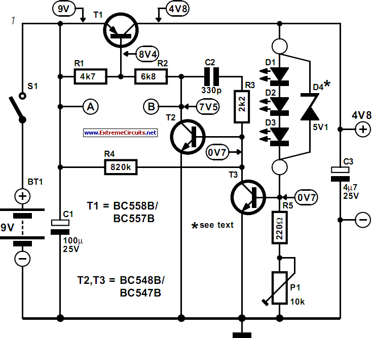
Therefore, a 9 V battery can be discharged to about 5 V, which is quite an improvement on the situation with an integrated regulator. Diodes D1-D2-D3, or a suitable zener diode (D4), in conjunction with R5 and P1, form a variable reference voltage source, which is used as the (output-dependent) base potential of T3. If the output voltage drops below a desired level, the base potential of T3 also drops. The transistor then conducts less hard and its collector voltage rises. The base voltage of T2 also rises, so that T1 is driven harder. This results in the near-instantaneous restoration of the output voltage.
The design of the reference voltage source is clearly of paramount importance. The current through the LEDs or the zener diode is of the order of only 100 µA. This means that thedrop across a 5.1 V zener diode is only 4.3 V and across each LED, only about 1.43 V. For a wanted output voltage of 4.8 V, the three LEDs proved very effective, whereas the zener did not. It may well be necessary, if a zener diode is used, to try one rated at 4.7 V. If, however, an output voltage of 5 V is wanted, it will be necessary to carefully select a zener diode. When the battery voltage has dropped to a level where it is only marginally higher than the wanted output voltage, T1 and T2 conduct hard.
A further drop in the battery voltage will cause the collector potential of T2 to drop rapidly to 0 V, since T2 tries to make T1 conduct hard. The large drop in the collector potential of T2 may be used to drive a BATT-LOW indicator. This may be done in three ways as shown in Figure 2. When network a is connected between terminals A and B, transistor T4 will normally be held cut off by divider R6-R7a. If then the voltage at B drops suddenly, T4 conducts, where-upon D5 indicates that the battery is nearly flat. The network in b is similar to that in a, but is intended for a liquid-crystal display of BATT-LOW.
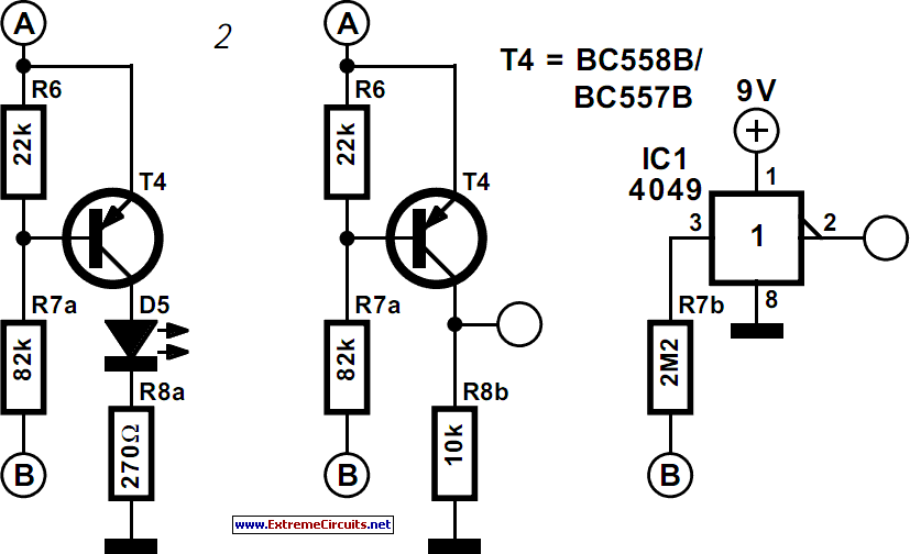
The collector of T4 is linked to the IC that drives the decimal point and the BAT-LOW segment of the display. Network c may be used if there is an unused inverter or gate in the circuit to be powered. The high value of resistor R7b prevents the internal protection diodes of the IC being damaged. When the regulator has been built, connect it to a variable power supply via a multimeter set to the mA range and set P1 roughly at its mid-position. Turn P1 slowly until the desired output voltage is obtained.
If with an output voltage of 4.8 V the regulator draws a current of more than 250–300 µA, the three LEDs or zener diode must be replaced. The regulator can provide a current of up to about 25 mA. With a fresh 9 V battery, the dissipation of T1 does not exceed 100 mW. If the input voltage is higher, it may be necessary to mount the transistor on a suitable heat sink or replace it by a power transistor, for instance, a Type BD138.