Junction field-effect transistors
The field effect transistor was proposed by Julius Lilienfeld in US patents in 1926 and 1933 (1,900,018). Moreover, Shockley, Brattain, and Bardeen were investigating the field effect transistor in 1947. Though, the extreme difficulties sidetracked them into inventing the bipolar transistor instead. Shockley's field effect transistor theory was published in 1952. However, the materials processing technology was not mature enough until 1960 when John Atalla produced a working device.
A field effect transistor (FET) is a unipolar device, conducting a current using only one kind of charge carrier. If based on an N-type slab of semiconductor, the carriers are electrons. Conversely, a P-type based device uses only holes.
At the circuit level, field effect transistor operation is simple. A voltage applied to the gate, input element, controls the resistance of the channel, the unipolar region between the gate regions. (Figure below) In an N-channel device, this is a lightly doped N-type slab of silicon with terminals at the ends. The source and drain terminals are analogous to the emitter and collector, respectively, of a BJT. In an N-channel device, a heavy P-type region on both sides of the center of the slab serves as a control electrode, the gate. The gate is analogous to the base of a BJT.
“Cleanliness is next to godliness” applies to the manufacture of field effect transistors. Though it is possible to make bipolar transistors outside of a clean room, it is a necessity for field effect transistors. Even in such an environment, manufacture is tricky because of contamination control issues. The unipolar field effect transistor is conceptually simple, but difficult to manufacture. Most transistors today are a metal oxide semiconductor variety (later section) of the field effect transistor contained within integrated circuits. However, discrete JFET devices are available.
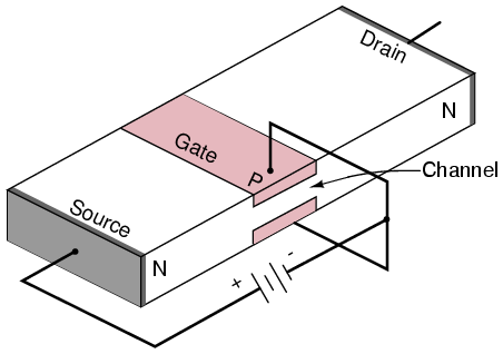
Junction field effect transistor cross-section.
A properly biased N-channel junction field effect transistor (JFET) is shown in Figure above. The gate constitutes a diode junction to the source to drain semiconductor slab. The gate is reverse biased. If a voltage (or an ohmmeter) were applied between the source and drain, the N-type bar would conduct in either direction because of the doping. Neither gate nor gate bias is required for conduction. If a gate junction is formed as shown, conduction can be controlled by the degree of reverse bias.
Figure below(a) shows the depletion region at the gate junction. This is due to diffusion of holes from the P=type gate region into the N-type channel, giving the charge separation about the junction, with a non-conductive depletion region at the junction. The depletion region extends more deeply into the channel side due to the heavy gate doping and light channel doping.
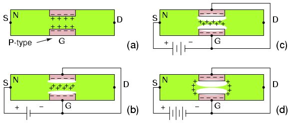
N-channel JFET: (a) Depletion at gate diode. (b) Reverse biased gate diode increases depletion region. (c) Increasing reverse bias enlarges depletion region. (d) Increasing reverse bias pinches-off the S-D channel.
The thickness of the depletion region can be increased Figure above(b) by applying moderate reverse bias. This increases the resistance of the source to drain channel by narrowing the channel. Increasing the reverse bias at (c) increases the depletion region, decreases the channel width, and increases the channel resistance. Increasing the reverse bias VGS at (d) will pinch-off the channel current. The channel resistance will be very high. This VGS at which pinch-off occurs is VP, the pinch-off voltage. It is typically a few volts. In summation,the channel resistance can be controlled by the degree of reverse biasing on the gate.
The source and drain are interchangeable, and the source to drain current may flow in either direction for low level drain battery voltage (< 0.6 V). That is, the drain battery may be replaced by a low voltage AC source. For a high drain power supply voltage, to 10's of volts for small signal devices, the polarity must be as indicated in Figure below(a). This drain power supply, not shown in previous figures, distorts the depletion region, enlarging it on the drain side of the gate. This is a more correct representation for common DC drain supply voltages, from a few to tens of volts. As drain voltage VDS is increased,the gate depletion region expands toward the drain. This increases the length of the narrow channel, increasing its resistance a little. We say "a little" because large resistance changes are due to changing gate bias. Figure below(b) shows the schematic symbol for an N-channel field effect transistor compared to the silicon cross-section at (a). The gate arrow points in the same direction as a junction diode. The“pointing” arrow and “non-pointing” bar correspond to P and N-type semiconductors, respectively.
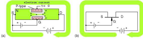
N-channel JFET electron current flow from source to drain in (a) cross-section, (b) schematic symbol.
Figure above shows a large electron current flow from (-) battery terminal, to FET source, out the drain, returning to the (+) battery terminal. This current flow may be controlled by varying the gate voltage. A load in series with the battery sees an amplified version of the changing gate voltage.
P-channel field effect transistors are also available. The channel is made of P-type material. The gate is a heavy N-type region. All the voltage sources are reversed in the P-channel circuit (Figure below) as compared with the more popular N-channel device. Also note, the arrow points out of the gate of the schematic symbol (b) of the P-channel field effect transistor.
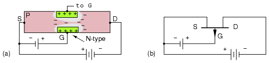
P-channel JFET: (a) N-type gate, P-type channel, reversed voltage sources compared with N-channel device. (b) Note reversed gate arrow and voltage sources on schematic.
As the positive gate bias voltage is increased, the resistance of the P-channel increases, decreasing the current flow in the drain circuit.
Discrete devices are manufactured with the cross-section shown in Figure below. The cross-section, oriented so that it corresponds to the schematic symbol, is upside down with respect to a semiconductor wafer. That is, the gate connections are on the top of the wafer. The gate is heavily doped, P+, to diffuse holes well into the channel for a large depletion region. The source and drain connections in this N-channel device are heavily doped, N+ to lower connection resistance. However, the channel surrounding the gate is lightly doped to allow holes from the gate to diffuse deeply into the channel. That is the N- region.
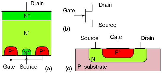
Junction field effect transistor: (a) Discrete device cross-section, (b) schematic symbol, (c) integrated circuit device cross-section.
All three FET terminals are available on the top of the die for the integrated circuit version so that a metalization layer (not shown) can interconnect multiple components. (Figure above(c) ) Integrated circuit FET's are used in analog circuits for the high gate input resistance.. The N-channel region under the gate must be very thin so that the intrinsic region about the gate can control and pinch-off the channel. Thus, gate regions on both sides of the channel are not necessary.
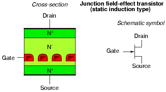
Junction field effect transistor (static induction type): (a) Cross-section, (b) schematic symbol.
The static induction field effect transistor (SIT) is a short channel device with a buried gate. (Figure above) It is a power device, as opposed to a small signal device. The low gate resistance and low gate to source capacitance make for a fast switching device. The SIT is capable of hundreds of amps and thousands of volts. And, is said to be capable of an incredible frequency of 10 gHz.[YYT]
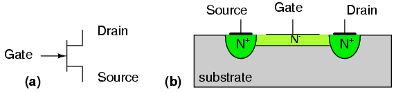
Metal semiconductor field effect transistor (MESFET): (a) schematic symbol, (b) cross-section.
The Metal semiconductor field effect transistor (MESFET) is similar to a JFET except the gate is a schottky diode instead of a junction diode. A schottky diode is a metal rectifying contact to a semiconductor compared with a more common ohmic contact. In Figure above the the source and drain are heavily doped (N+). The channel is lightly doped (N-). MESFET's are higher speed than JFET's. The MESET is a depletion mode device, normally on, like a JFET. They are used as microwave power amplifiers to 30 gHz. MESFET's can be fabricated from silicon, gallium arsenide, indium phosphide, silicon carbide, and the diamond allotrope of carbon.
- REVIEW:
- The unipolar junction field effect transistor (FET or JFET) is so called because conduction in the channel is due to one type of carrier
- The JFET source, gate, and drain correspond to the BJT's emitter, base, and collector, respectively.
- Application of reverse bias to the gate varies the channel resistance by expanding the gate diode depletion region.