Analog-to-Digital conversion
Question 1:
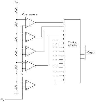
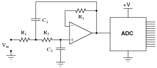
The circuit shown here is a four-bit analog-to-digital converter (ADC). Specifically, it is a flash converter, so named because of its high speed:
|
|
Explain why we must use a priority encoder to encode the comparator outputs into a four-bit binary code, and not a regular encoder. What problem(s) would we have if we were to use a non-priority encoder in this ADC circuit?
Notes:
Here, I show students a very practical application of a priority encoder, in which the necessity of priority encoding should be apparent after some analysis of the circuit.
Question 2:
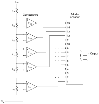
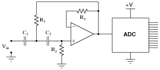
Predict how the operation of this "flash" analog-to-digital converter (ADC) circuit will be affected as a result of the following faults. Consider each fault independently (i.e. one at a time, no multiple faults):
|
|
- �
- Resistor R16 fails open:
- �
- Resistor R1 fails open:
- �
- Comparator U13 output fails low:
- �
- Solder bridge (short) across resistor R14:
For each of these conditions, explain why the resulting effects will occur.
- �
- Resistor R16 fails open: Output code will be 15 (1111) all the time.
- �
- Resistor R1 fails open: If Vin < Vref, output will be 0 (0000); if Vin > Vref, output will be 15 (1111).
- �
- Comparator U13 output fails low: Output will assume the "13" state (1101) unless Vin exceeds that analog value, then the ADC will register properly.
- �
- Solder bridge (short) across resistor R14: There will be no distinctive "13" state (1101), the analog values for all the other states adjusting slightly to fill the gap.
Notes:
The purpose of this question is to approach the domain of circuit troubleshooting from a perspective of knowing what the fault is, rather than only knowing what the symptoms are. Although this is not necessarily a realistic perspective, it helps students build the foundational knowledge necessary to diagnose a faulted circuit from empirical data. Questions such as this should be followed (eventually) by other questions asking students to identify likely faults based on measurements.
Question 3:
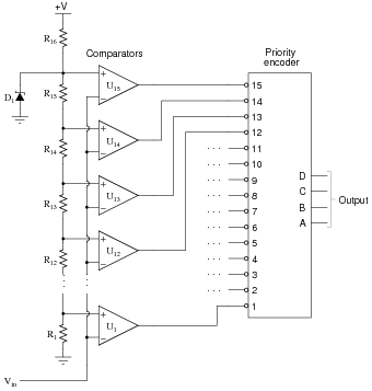
This "flash" ADC circuit has a problem. The output code jumps from 0000 to 1111 with just the slightest amount of input voltage (Vin). In fact, the only time it outputs 0000 is when the input terminal is slightly negative with reference to ground:
|
|
Identify at least two possible component faults that could cause this problem, and explain your reasoning in how you made the identifications.
Notes:
Have your students explain their reasoning in class to you, so that you may observe their diagnostic thought processes.
Question 4:
| Don't just sit there! Build something!! |
Learning to analyze digital circuits requires much study and practice. Typically, students practice by working through lots of sample problems and checking their answers against those provided by the textbook or the instructor. While this is good, there is a much better way.
You will learn much more by actually building and analyzing real circuits, letting your test equipment provide the änswers" instead of a book or another person. For successful circuit-building exercises, follow these steps:
- 1.
- Draw the schematic diagram for the digital circuit to be analyzed.
- 2.
- Carefully build this circuit on a breadboard or other convenient medium.
- 3.
- Check the accuracy of the circuit's construction, following each wire to each connection point, and verifying these elements one-by-one on the diagram.
- 4.
- Analyze the circuit, determining all output logic states for given input conditions.
- 5.
- Carefully measure those logic states, to verify the accuracy of your analysis.
- 6.
- If there are any errors, carefully check your circuit's construction against the diagram, then carefully re-analyze the circuit and re-measure.
Always be sure that the power supply voltage levels are within specification for the logic circuits you plan to use. If TTL, the power supply must be a 5-volt regulated supply, adjusted to a value as close to 5.0 volts DC as possible.
One way you can save time and reduce the possibility of error is to begin with a very simple circuit and incrementally add components to increase its complexity after each analysis, rather than building a whole new circuit for each practice problem. Another time-saving technique is to re-use the same components in a variety of different circuit configurations. This way, you won't have to measure any component's value more than once.
Notes:
It has been my experience that students require much practice with circuit analysis to become proficient. To this end, instructors usually provide their students with lots of practice problems to work through, and provide answers for students to check their work against. While this approach makes students proficient in circuit theory, it fails to fully educate them.
Students don't just need mathematical practice. They also need real, hands-on practice building circuits and using test equipment. So, I suggest the following alternative approach: students should build their own "practice problems" with real components, and try to predict the various logic states. This way, the digital theory "comes alive," and students gain practical proficiency they wouldn't gain merely by solving Boolean equations or simplifying Karnaugh maps.
Another reason for following this method of practice is to teach students scientific method: the process of testing a hypothesis (in this case, logic state predictions) by performing a real experiment. Students will also develop real troubleshooting skills as they occasionally make circuit construction errors.
Spend a few moments of time with your class to review some of the "rules" for building circuits before they begin. Discuss these issues with your students in the same Socratic manner you would normally discuss the worksheet questions, rather than simply telling them what they should and should not do. I never cease to be amazed at how poorly students grasp instructions when presented in a typical lecture (instructor monologue) format!
I highly recommend CMOS logic circuitry for at-home experiments, where students may not have access to a 5-volt regulated power supply. Modern CMOS circuitry is far more rugged with regard to static discharge than the first CMOS circuits, so fears of students harming these devices by not having a "proper" laboratory set up at home are largely unfounded.
A note to those instructors who may complain about the "wasted" time required to have students build real circuits instead of just mathematically analyzing theoretical circuits:
What is the purpose of students taking your course?
If your students will be working with real circuits, then they should learn on real circuits whenever possible. If your goal is to educate theoretical physicists, then stick with abstract analysis, by all means! But most of us plan for our students to do something in the real world with the education we give them. The "wasted" time spent building real circuits will pay huge dividends when it comes time for them to apply their knowledge to practical problems.
Furthermore, having students build their own practice problems teaches them how to perform primary research, thus empowering them to continue their electrical/electronics education autonomously.
In most sciences, realistic experiments are much more difficult and expensive to set up than electrical circuits. Nuclear physics, biology, geology, and chemistry professors would just love to be able to have their students apply advanced mathematics to real experiments posing no safety hazard and costing less than a textbook. They can't, but you can. Exploit the convenience inherent to your science, and get those students of yours practicing their math on lots of real circuits!
Question 5:
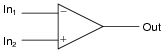
A comparator may be thought of as a one-bit analog-to-digital converter:
|
|
Explain why this description of a comparator is appropriate. What exactly is meant by the term änalog-to-digital converter," or ADC?
Notes:
This description of a comparator is not just theoretical. In many practical ADC circuits, a comparator is actually used as the primary analog-to-digital conversion device. This is particularly true for oversampling or Sigma-Delta converters, which may be built around a single (1-bit) comparator.
Question 6:
Flash analog-to-digital converters are easy to understand, but are not practical for many applications. Identify some of the drawbacks of the "flash" circuit design.
Notes:
It is a shame that flash converter circuits suffer the disadvantage(s) that they do. They are so simple to understand and have such an inherent speed advantage over other circuit designs! Discuss with your students why the weaknesses of the flash design make the other ADC types necessary, and even preferable in most applications.
Question 7:
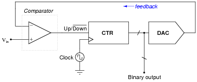
Explain the operating principle of this analog-to-digital converter circuit, usually referred to as a tracking converter:
|
|
Follow-up question: this form of ADC is not very effective at following fast-changing input signals. Explain why.
Notes:
Have your students express the answer to this question in their own words, not just copying the answer I provide. Aside from the flash converter, the tracking converter is one of the easiest ADC circuits to understand.
Question 8:
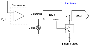
Explain the operating principle of this analog-to-digital converter circuit, usually referred to as a successive-approximation converter:
|
|
Note: the successive-approximation register (SAR) is a special type of binary counting circuit which begins counting with the most-significant bit (MSB), then the next-less-significant bit, in order all the way down to the LSB. At that point, it outputs a "high" signal at the "Complete" output terminal. The operation of this register may be likened to the manual process of converting a decimal number to binary by "trial and fit" with the MSB first, through all the successive bits down to the LSB.
Follow-up question: this form of ADC is much more effective at following fast-changing input signals than the tracking converter design. Explain why.
Notes:
Have your students express the answer to this question in their own words, not just copying the answer I provide. Aside from the flash converter, the tracking converter is one of the easiest ADC circuits to understand.
Question 9:
Explain the operating principle of a single-slope ADC circuit, in your own words.
Notes:
Tutorials abound on simple ADC strategies, so your students should have little problem locating an adequate explanation for the operation of a single-slope ADC.
Question 10:
Explain the operating principle of a dual-slope ADC circuit, in your own words.
Notes:
Tutorials abound on simple ADC strategies, so your students should have little problem locating an adequate explanation for the operation of a dual-slope ADC.
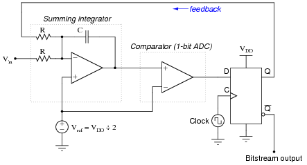
Question 11:
The Delta-Sigma or Sigma-Delta analog-to-digital converter works on the principle of oversampling, whereby a low-resolution ADC repeatedly samples the input signal in a feedback loop. In many cases, the ADC used is nothing more than a comparator (a 1-bit ADC!), the output of this ADC subtracted from the input signal and integrated over time in an attempt to achieve a balance near 0 volts at the output of the integrator. The result is a pulse-density modulated (PDM) "bitstream" of 1-bit digital data which may be filtered and decimated (converted to a binary word of multiple bits):
|
|
Explain what this PDM bitstream would look like for the following input voltage conditions:
- �
- Vin = 0 volts
- �
- Vin = VDD
- �
- Vin = Vref
- �
- Vin = 0 volts ; bitstream = 00000000 . . .
- �
- Vin = VDD ; bitstream = 11111111 . . .
- �
- Vin = Vref ; bitstream = 01010101 . . .
Notes:
In order to answer this question, students must have a good grasp of how the summing integrator works. Discuss with them how the feedback loop's "goal" is to maintain the integrator output at the reference voltage (Vref), and how the 1-bit ADC can only make adjustments to the integrator's output by driving it upward or downward by the same analog quantity every clock pulse.
Question 12:
The pulse-density modulation (PDM) of a 1-bit oversampled Delta-Sigma modulator circuit may be "decimated" into a multi-bit binary number simply by counting the number of "1" states in a bitstream of fixed length.
Take for example the following bitstreams. Sample the first seven bits of each stream, and convert the equivalent binary numbers based on the number of "high" bits in each seven-bit sample:
- �
- 001001001001001
- �
- 101101101101101
- �
- 010010001100010
- �
- 010001100010001
- �
- 111011101110111
Then, take the same five PDM bitstreams and "decimate" them over a sampling interval of 15 bits.
- �
- 001001001001001 ; Binary value = 0102
- �
- 101101101101101 ; Binary value = 1012 or 1002
- �
- 010010001100010 ; Binary value = 0102 or 0112
- �
- 010001100010001 ; Binary value = 0112 or 0012
- �
- 111011101110111 ; Binary value = 1102 or 1012
Sampling interval = 15 bits
- �
- 001001001001001 ; Binary value = 01012
- �
- 101101101101101 ; Binary value = 10102
- �
- 010010001100010 ; Binary value = 01012
- �
- 010001100010001 ; Binary value = 01012
- �
- 111011101110111 ; Binary value = 11002
Follow-up question: what relationship do you see between sampling speed and resolution in this "decimation" process, and how does this relate to the performance of a Delta-Sigma ADC?
Notes:
With little effort, your students should be able to see that sampling twice as many bits in the PDM bitstream adds one more bit of resolution to the final binary output. Such is the nature of so many circuits: that optimization of one performance parameter comes at the expense of another.
Students may question how two (or more!) different decimation results can occur from the same bitstream, especially as shown in the answer for the 7-bit groupings. The answer is two-part: first, the bitstreams I show are not all perfectly repetitive. Some change pattern (slightly) mid-way, which leads to different pulse densities in different sections. The second part to this answer is that the nature of decimation by grouping will inevitably lead to differing results (even when the pattern is perfectly repetitive), and that this is the converter's "way" of resolving an analog quantity lying between two discrete output states. In other words, a pair of decimated values of "4" and "5" (1002 and 1012, respectively) from a perfectly repetitive bitstream suggests an analog value lying somewhere between the discrete integer values of "4" and "5". Only by sampling groups of bits equal to the period of the PDM repetition (or integer multiples of that
repetition) can the digital output precisely and constantly equal the analog input.
Question 13:
Suppose an analog-digital converter IC ("chip") inputs a voltage ranging from 0 to 5 volts DC and converts the magnitude of that voltage into an 8-bit binary number. How many discrete ßteps" are there in the output as the converter circuit resolves the input voltage from one end of its range (0 volts) to the other (5 volts)? How much voltage does each of these steps represent?
Notes:
This question is not so much about ADC circuitry as it is about digital resolution in general. Any digital system with a finite number of parallel bits has a finite range. When representing analog variables in digital form by the limited number of bits available, there will be a certain minimum voltage increment represented by each ßtep" in the digital output. Here, students get to see how the discrete nature of a binary number translates to real-life measurement "rounding."
Question 14:
One of the idiosyncrasies of analog-to-digital conversion is a phenomenon known as aliasing. It happens when an ADC attempts to digitize a waveform with too high of a frequency.
Explain what aliasing is, how it happens, and what may be done to prevent it from happening to an ADC circuit.
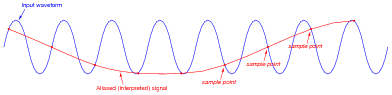
|
|
Notes:
The point of this question (and of the answer given) is to have students put this important concept into their own words.
Something noteworthy for students and instructors alike is that aliasing may be visually experienced using digital oscilloscopes. Setting the timebase (seconds/division) control too slow may result in a false (aliased) waveform displayed in the oscilloscope. Not only does this make a good classroom demonstration, but it also is a great lesson to learn if one expects to use digital oscilloscopes on a regular basis!
Question 15:
Analog-to-digital converter circuits (ADC) are usually equipped with analog low-pass filters to pre-condition the signal prior to digitization. This prevents signals with frequencies greater than the sampling rate from being seen by the ADC, causing a detrimental effect called aliasing. These analog pre-filters are thus known as anti-aliasing filters.
Determine which of the following Sallen-Key active filters is of the correct type to be used as an anti-aliasing filter:
|
|
|
|
Notes:
Discuss with your students various ways of identifying active filter types. What clues are present in these two circuits to reveal their filtering characteristics?
Question 16:
Suppose a particular ADC has an input voltage range of +5 volts to -5 volts, and therefore is suitable for digitizing AC input signals. A technician wants to use this ADC to digitize AC line voltage (120 volts RMS), and builds the following conditioning circuit to safely connect the ADC to the AC line:
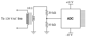
|
|
Unfortunately, this ADC is not able to fully sample the AC waveform when tested. It överflows" and ünderflows" at the waveform's peaks, as though the input waveform is too large (outside of the +5/-5 volt ADC chip range). The technician re-checks his calculations, but still thinks the voltage division ratio provided by the potential transformer and resistor network should be sufficient for this task.
What is wrong with this circuit? Why does it över-range" at the waveform peaks instead of sampling the 120 volt waveform with range to spare? Then, once having identified the problem, recommend a solution to fix the problem.
Challenge question: one thing the technician did right in this circuit was use a transformer as the front-end of his signal conditioning network. Explain why this was a smart idea. In other words, why would it possibly be worse to simply use a resistive voltage divider to do all the attenuation, instead of using a step-down transformer to do part of it and a resistive divider to do the rest?
Notes:
The given answer is purposefully minimal, but should contain enough information that anyone familiar with RMS versus peak sinusoidal values should realize what the problem is. There is more than one practical solution for fixing this problem, so be sure to allow time for discussion into the various options.
Question 17:
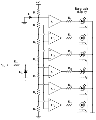
This bargraph driver circuit takes an audio input signal and displays the amplitude as a moving "bar" of lights. The stronger the amplitude of the signal, the more LEDs energize in the bargraph display. Predict how the operation of this circuit will be affected as a result of the following faults. Consider each fault independently (i.e. one at a time, no multiple faults):
|
|
- �
- Resistor R4 failed open:
- �
- Solder bridge (short) past resistor R3:
- �
- Resistor R11 failed open:
- �
- Zener diode D1 failed shorted:
- �
- Schottky diode D2 failed shorted:
- �
- Resistor R4 failed open: LEDs 1 through 3 always off, LEDs 4 through 6 always on (with any substantial input signal amplitude at all).
- �
- Solder bridge (short) past resistor R3: LEDs 2 and 3 always energize at the same time.
- �
- Resistor R11 failed open: LED 4 never lights up.
- �
- Zener diode D1 failed shorted: All LEDs light up together with any substantial input signal amplitude at all.
- �
- Schottky diode D2 failed shorted: None of the LEDs ever light up.
Follow-up question: does each comparator source or sink current to its respective LED?
Challenge question: if resistors R1 through R7 are all equal value, the response of the bargraph will be linear (twice the signal amplitude results in twice as many LEDs energized). What would have to be changed in this circuit to give the bargraph a logarithmic response, so it registered proportional to a decibel scale rather than a voltage scale?
Notes:
Questions like this help students hone their troubleshooting skills by forcing them to think through the consequences of each possibility. This is an essential step in troubleshooting, and it requires a firm understanding of circuit function.
Question 18:
Examine this vertical ("bird's eye") view of a boat resisting a river's current:

|
|
Suppose the driver of this boat does not own an anchor, and furthermore that the only form of propulsion is an electric "trolling" motor with an on/off switch (no variable speed control). With the right combination of switch actuations (on, off, on, off), it should be possible for the boat to maintain its position relative to the riverbanks, against the flow of water.
Now, if we know the boat is actually holding position in the middle of the river, by trolling motor power alone, the pattern of on/off switch actuations should tell us something about the speed of the river. Perform a couple of "thought experiments" where you imagine what the driver of the boat would have to do with the motor's on/off switch to maintain position against a fast current, versus against a slow current. What relationship do you see between the switch actuations and the speed of the current?
Note: once you understand this question, you will be better prepared to grasp the operation of a Delta-Sigma analog-to-digital converter!
Notes:
The purpose of this question is to present an analogy which students may use to grasp the operation of a Delta-Sigma ADC: the idea that a bitstream (PDM) may represent an analog value.