Performance-based assessments for digital circuit competencies
Question 1:
| (Template) |
|
|
Notes:
Any relevant notes for the assessment activity go here.
Question 2:
|
|
Notes:
An extension of this exercise is to incorporate troubleshooting questions. Whether using this exercise as a performance assessment or simply as a concept-building lab, you might want to follow up your students' results by asking them to predict the consequences of certain circuit faults.
Question 3:
|
|
Notes:
An extension of this exercise is to incorporate troubleshooting questions. Whether using this exercise as a performance assessment or simply as a concept-building lab, you might want to follow up your students' results by asking them to predict the consequences of certain circuit faults.
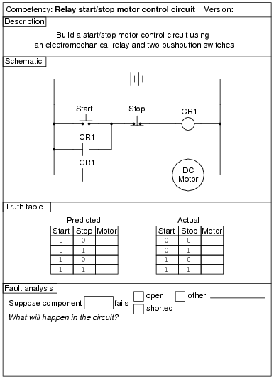
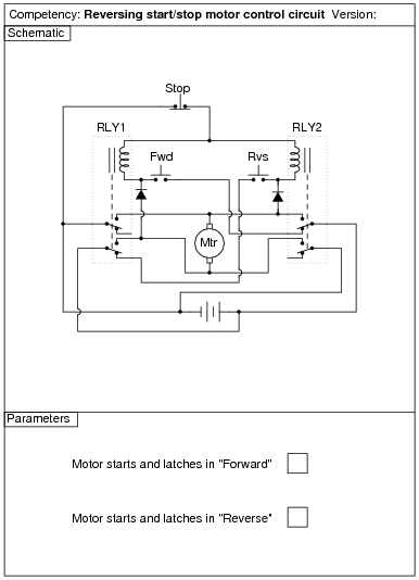
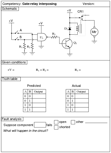
The two diodes in this circuit are a matter of necessity: getting the circuit to work with only two sets of switch contacts per relay. Ideally, each relay would be 3PDT with separate contact sets for latching, interlocking, and motor power. To use a DPDT relay requires that one of these contact sets do double-duty. In this case, one of the contact sets on each relay handling power to the motor must also handle the job of seal-in (latching). Without the diodes in place, both relays chatter when either motion button is pressed. This is because both relay coils receive power: one coil directly through the switch; the other through the same switch, back through the motor, and then through the seal-in (latching) connection. The diodes prevent this "feed-through" to the other relay coil from happening, without interfering with the normal latching function.
Question 4:
|
|
Notes:
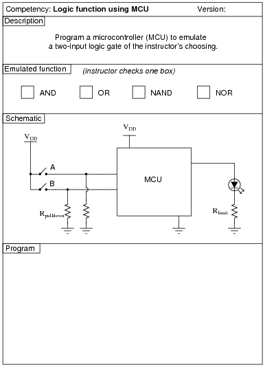
Here, I let students choose appropriate values for Rpulldown and Rlimit, rather than specify them as given conditions.
Question 5:
|
|
Notes:
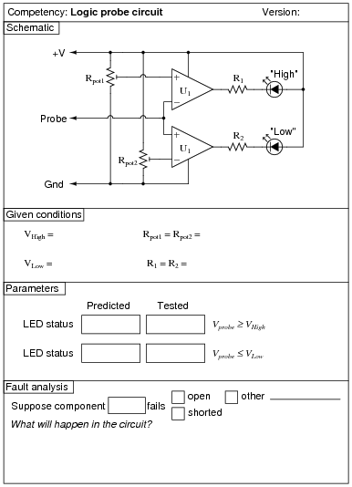
I recommend the use of the LM339 comparator for this circuit.
An extension of this exercise is to incorporate troubleshooting questions. Whether using this exercise as a performance assessment or simply as a concept-building lab, you might want to follow up your students' results by asking them to predict the consequences of certain circuit faults.
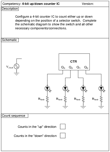
Question 6:
|
|
Notes:
The choice of diodes is not critical in a circuit where the inputs come from manually actuated switches. Neither is the choice of resistor sizes (10 kW) works just fine, especially when the only thing loading the output is the student's logic probe or voltmeter.
Question 7:
|
|
Notes:
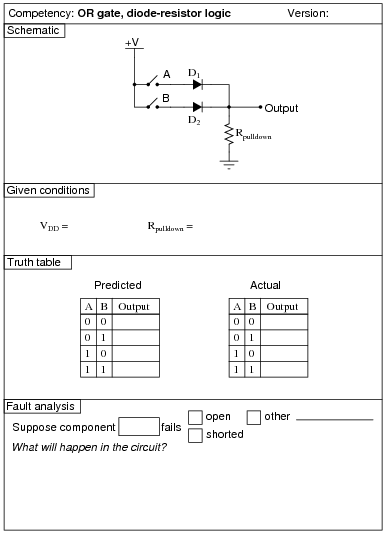
It should be noted that the input states in this circuit are defined by the voltage levels, not by the contact status. In other words, a closed contact equals a "low" (0) logic state.
The choice of diodes is not critical in a circuit where the inputs come from manually actuated switches. Neither is the choice of resistor sizes (10 kW) works just fine, especially when the only thing loading the output is the student's logic probe or voltmeter.
Question 8:
|
|
Notes:
Nothing special to note here!
Question 9:
|
|
Notes:
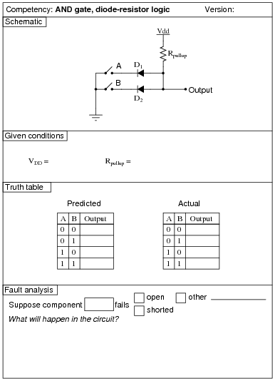
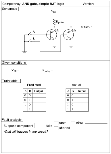
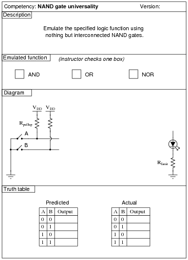
It needs to be understood that this is an AND gate only if you consider the "0" and "1" states as defined by voltage levels with respect to ground, and not by switch actuation. Many students assume an actuated (pushed) switch is a "1" input and a de-actuated (unpushed) switch is a "0" input. Not necessarily so! In this circuit, the switches are connecting inputs to ground. This means a closed (actuated) switch provides a low (0) input state, while an open (unactuated) switch provides a high (1) input state.
Question 10:
|
|
Notes:
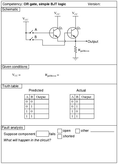
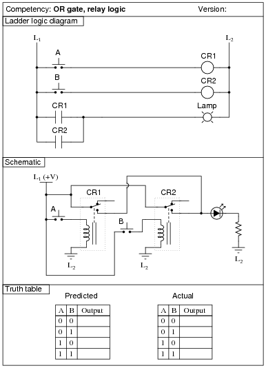
The transition from ladder logic diagram to actual relay wiring is a confusing one for many students. This is what I consider to be the most significant learning objective of this exercise: figuring out how to build the circuit, not necessarily understanding the logical function of it.
Question 11:
|
|
Notes:
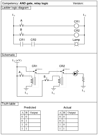
The transition from ladder logic diagram to actual relay wiring is a confusing one for many students. This is what I consider to be the most significant learning objective of this exercise: figuring out how to build the circuit, not necessarily understanding the logical function of it.
Question 12:
|
|
Notes:
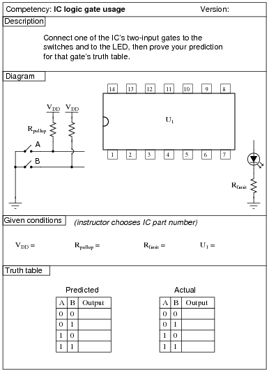
The purpose of this exercise is for students to research what type of IC this is (from the given part number for U1), its pinout, and then predict and prove its operation using truth tables to document the results. You, as the instructor, may select any 14-pin CMOS or TTL logic IC that you wish. Students are to draw the logic gate symbol within the rectangle of U1, then connect that symbol to the input switches and output LED.
It needs to be understood that the "0" and "1" states are defined by voltage levels with respect to ground, and not by switch actuation. Many students assume an actuated (pushed) switch is a "1" input and a de-actuated (unpushed) switch is a "0" input. Not necessarily so! In this circuit, the switches are connecting inputs to ground. This means a closed (actuated) switch provides a low (0) input state, while an open (unactuated) switch provides a high (1) input state.
Question 13:
|
|
Notes:
Something omitted from too many basic digital electronics texts is a thorough discussion on interfacing IC logic gates with high-power devices, usually using relays. This is a very important subject, however, because many devices we wish to control with digital logic circuits are too power-hungry to directly drive with the logic gate outputs! Here, students get the opportunity to experiment with how to make a logic gate (CMOS, preferably) drive an electric motor.
One component value you may wish to have your students size themselves is resistor R3, being the base current limiting resistor for transistor Q1. It must be sized such that the transistor is saturated with the gate output in the HIGH state, yet not allowing so much base current that the transistor becomes damaged. Figuring out an appropriate size for this resistor is a very practical exercise, forcing students to review transistor theory (calculations with b) as well as consider characteristics of the load.
It may be advisable (especially if the logic gate is TTL and requires a precise 5.0 volt power supply) to have a separate source of power for the electric motor.
Question 14:
|
|
Notes:
It should be noted that the input states in this circuit are defined by the voltage levels, not by the contact status. In other words, a closed contact equals a "low" (0) logic state.
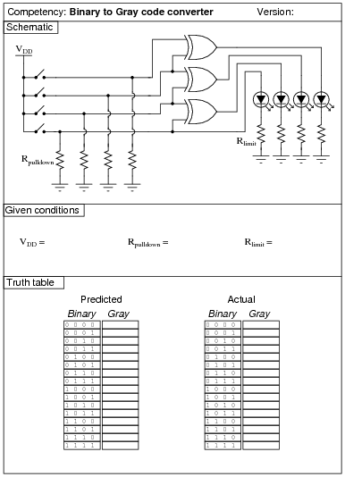
I strongly recommend having students build their logic circuits with CMOS chips rather than TTL, because of the less stringent power supply requirements of CMOS. I also recommend drawing a combinational circuit using four gates, because this is the common number of two-input gates found on 14-pin DIP logic chips.
Question 15:
|
|
Notes:
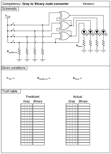
I strongly recommend having students build their logic circuits with CMOS chips rather than TTL, because of the less stringent power supply requirements of CMOS. I also recommend drawing a combinational circuit using four gates, because this is the common number of two-input gates found on 14-pin DIP logic chips.
Question 16:
|
|
Notes:
I strongly recommend having students build their logic circuits with CMOS chips rather than TTL, because of the less stringent power supply requirements of CMOS. I also recommend drawing a combinational circuit using four gates, because this is the common number of two-input gates found on 14-pin DIP logic chips.
Question 17:
|
|
Notes:
It should be noted that the input states in this circuit are defined by the voltage levels, not by the contact status. In other words, a closed contact equals a "low" (0) logic state.
I strongly recommend having students build their logic circuits with CMOS chips rather than TTL, because of the less stringent power supply requirements of CMOS. I also recommend drawing a combinational circuit using four gates, because this is the common number of two-input gates found on 14-pin DIP logic chips.
Question 18:
|
|
Notes:
It should be noted that the input states in this circuit are defined by the voltage levels, not by the contact status. In other words, a closed contact equals a "low" (0) logic state.
I strongly recommend having students build their logic circuits with CMOS chips rather than TTL, because of the less stringent power supply requirements of CMOS. I also recommend drawing a combinational circuit using four gates, because this is the common number of two-input gates found on 14-pin DIP logic chips.
Question 19:
|
|
Notes:
It should be noted that the input states in this circuit are defined by the voltage levels, not by the contact status. In other words, a closed contact equals a "low" (0) logic state.
I strongly recommend having students build their logic circuits with CMOS chips rather than TTL, because of the less stringent power supply requirements of CMOS. I also recommend drawing a combinational circuit using four gates, because this is the common number of two-input gates found on 14-pin DIP logic chips.
Question 20:
|
|
Notes:
It should be noted that the input states in this circuit are defined by the voltage levels, not by the contact status. In other words, a closed contact equals a "low" (0) logic state.
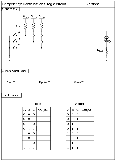
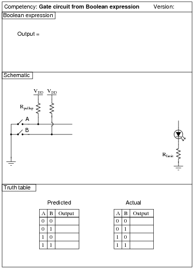
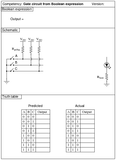
Here are some suggested Boolean expressions for your students to build gate circuits from:
- �
- Output = AB + A
- �
- Output = [`A]B + A
- �
- Output = (A + B)A
- �
- Output = (A + B)B
- �
- Output = [`A] + B
- �
- Output = A +[`B]
- �
- Output = [`A]B
- �
- Output = A[`B]
Question 21:
|
|
Notes:
It should be noted that the input states in this circuit are defined by the voltage levels, not by the contact status. In other words, a closed contact equals a "low" (0) logic state.
Here are some suggested Boolean expressions for your students to build gate circuits from:
- �
- Output = AB + C
- �
- Output = (A + B)C
- �
- Output = [`A] + BC
- �
- Output = [`A]B + C
Question 22:
|
|
Notes:
It should be noted that the input states in this circuit are defined by the voltage levels, not by the contact status. In other words, a closed contact equals a "low" (0) logic state.
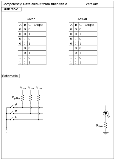
Suggested truth tables include the following (encoded as Boolean SOP statements):
- �
- AB[`C] + ABC
- �
- [`A]B[`C] +[`A]BC
- �
- [`A]B[`C] +[`A]BC +[`A] [`B] [`C]
- �
- A[`B] [`C] + A [`B] C
- �
- AB[`C] + A[`B] [`C] +[`A] [`B] [`C]
- �
- [`A]BC +[`A] [`B] C +[`A] [`B] [`C]
- �
- ABC +[`A]BC + AB[`C]
- �
- A[`B]C +[`A] [`B]C +[`A] [`B] [`C]
- �
- ABC + A[`B]C +[`A] [`B] C
I strongly recommend having students build their logic circuits with CMOS chips rather than TTL, because of the less stringent power supply requirements of CMOS. I also recommend drawing a combinational circuit using four gates, because this is the common number of two-input gates found on 14-pin DIP logic chips.
Question 23:
|
|
Notes:
It should be noted that the input states in this circuit are defined by the voltage levels, not by the contact status. In other words, a closed contact equals a "low" (0) logic state.
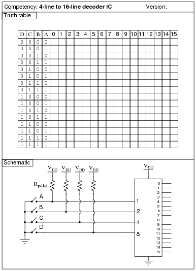
Here, the arrangement of the input letters D, C, B, and A is purposeful: D represents the most significant bit, while A represents the least significant bit, just like the IC datasheets typically order the input lines.
Normally, I draw LEDs in the schematic to give visual indication of output states. Here, due to the sheer number of required LEDs (16), I decided not to. However, students with access to lots of LEDs may choose to add them to their circuits, because visual indicators do make the circuit's function easier to understand.
If the decoder IC has enable inputs, the students must figure out what to do with them to make the circuit function!
Question 24:
|
|
Notes:
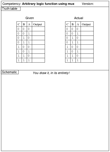
The purpose of this exercise is for students to connect a multiplexer to fulfill an arbitrary logic function specified by the instructor, thus showing the flexibility of the technique.
Here, the arrangement of the input letters C, B, and A is purposeful: C represents the most significant bit, while A represents the least significant bit, just like the IC datasheets typically order the input lines.
Question 25:
|
|
Notes:
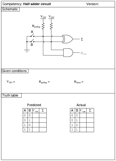
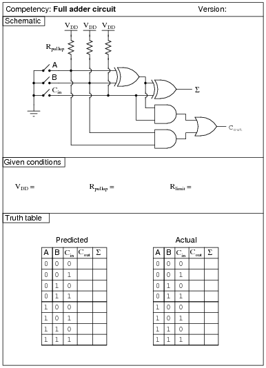
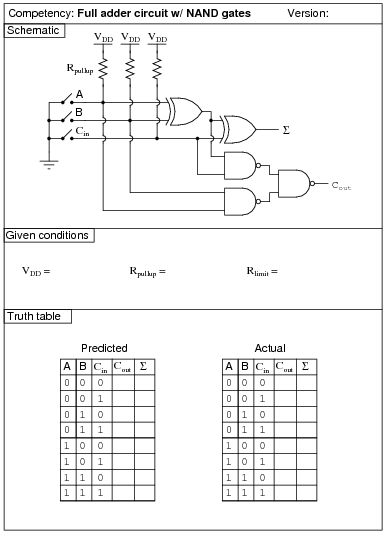
Here, I let students choose appropriate values for Rpullup and Rlimit, rather than specify them as given conditions.
Question 26:
|
|
Notes:
Here, I let students choose appropriate values for Rpullup and Rlimit, rather than specify them as given conditions.
Question 27:
|
|
Notes:
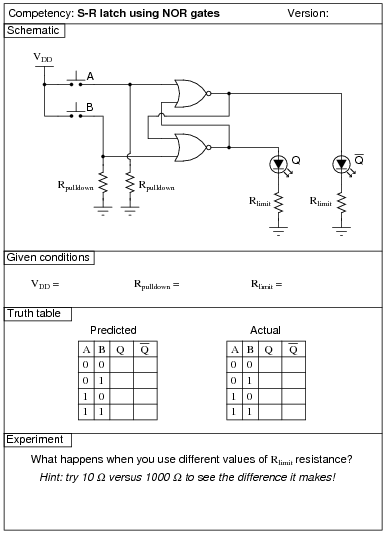
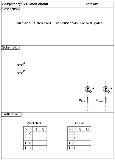
Pushbutton switches are recommended over toggle switches for demonstrating a latch circuit. When the contacts are momentary, the latching characteristics of the circuit becomes more evident to see.
I have intentionally requested students try different resistance values for Rlimit so they may see the effects of gate output loading, and the importance of proper logic level voltages. Students should try undersized resistors (10 W, perhaps) on both LEDs to generate this problem, and then use oversized resistors (1000 W, perhaps) to make the problem go away. Large-valued limiting resistors will cause the LEDs to be dim, but will also restore workable voltage levels so that "high" output states are actually interpreted as "high" when fed back to the gate inputs.
Question 28:
|
|
Notes:
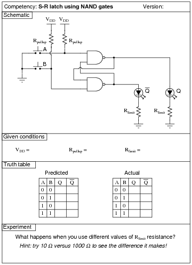
Pushbutton switches are recommended over toggle switches for demonstrating a latch circuit. When the contacts are momentary, the latching characteristics of the circuit becomes more evident to see.
I have intentionally requested students try different resistance values for Rlimit so they may see the effects of gate output loading, and the importance of proper logic level voltages. Students should try undersized resistors (10 W, perhaps) on both LEDs to generate this problem, and then use oversized resistors (1000 W, perhaps) to make the problem go away. Large-valued limiting resistors will cause the LEDs to be dim, but will also restore workable voltage levels so that "high" output states are actually interpreted as "high" when fed back to the gate inputs.
Question 29:
|
|
Notes:
Pushbutton switches are recommended over toggle switches for demonstrating a latch circuit. When the contacts are momentary, the latching characteristics of the circuit becomes more evident to see.
If students use LEDs to indicate the Q and [`Q] output states, they may experience trouble with the circuit not latching as it should. This is an excellent example of gate output loading, and the importance of proper logic level voltages. If such problems are encountered, advise the student(s) to use over-sized (too large) LED dropping resistors. This will cause the LEDs to be dim, but restore workable voltage levels so that "high" output states are actually interpreted as "high" when fed back to the gate inputs.
Question 30:
|
|
Notes:
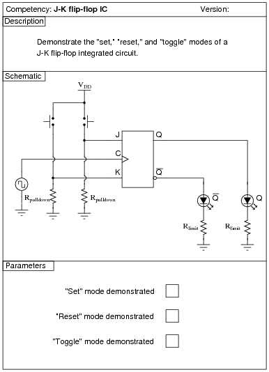
In this activity, students are asked to figure out how to wire the inputs of the J-K flip-flop circuit, and also how to demonstrate the three modes (Set, Reset, and Toggle). Students will have to properly set up their square-wave signal generators to create a workable clock pulse. This not only means a clock pulse at the correct voltage levels, but also one that is slow enough to allow them to clearly see the toggling of the flip-flop.
A great thing to do here is have students use a logic probe to sense the clock pulse and compare that frequency with the blinking of the Q and [`Q] LEDs.
Question 31:
|
|
Notes:
One lesson of digital circuits many students learn the hard way is the importance of not leaving CMOS inputs floating. In this case, the lesson is often learned in the form of leaving asynchronous inputs of the J-K flip-flops floating (preset, clear, or both). Be sure to check to see that all chip inputs are accounted for before passing students on this competency. If you see an input floating, touch the chip pin with a pen or pencil and let your students see the effect static has on their circuit!
Question 32:
|
|
Notes:
I strongly recommend having students build their logic circuits with CMOS chips rather than TTL, because of the less stringent power supply requirements of CMOS.
Question 33:
|
|
Notes:
Students are to research the datasheet for their particular IC and figure out from that what connections and timing sequences they need to make the circuit perform as requested. It is very important for students to learn to interpret manufacturers' datasheets!
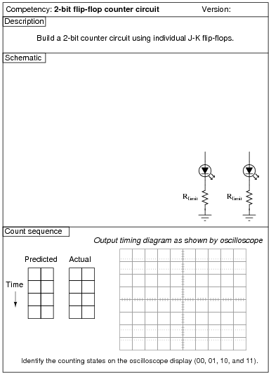
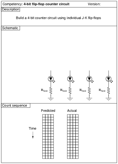
I recommend a slow clock frequency (1 Hz or so) to allow for easy viewing of the count sequence.
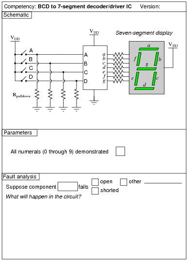
Question 34:
|
|
Notes:
Students are left on their own to figure out what they must do with the other inputs (lamp test, BI, RBI, etc.) to make the decoder/driver chip function properly.
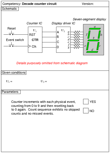
Question 35:
|
|
Notes:
I have purposely left the details of the schematic diagram vague, so that students must do a lot of datasheet research on their own to figure out how to make an event counter circuit. You may choose to give your students part numbers for the integrated circuits, or choose not to, depending on how capable your students are. The point is, they must figure out how to make the ICs work based on what they read from the manufacturer.
Something else students will probably have to do is de-bounce the event switch. Some event switches are inherently bounceless, while others are definitely not. Switch debouncing is something your students need to learn about and integrate into this circuit.
An extension of this exercise is to incorporate troubleshooting questions. Whether using this exercise as a performance assessment or simply as a concept-building lab, you might want to follow up your students' results by asking them to predict the consequences of certain circuit faults.
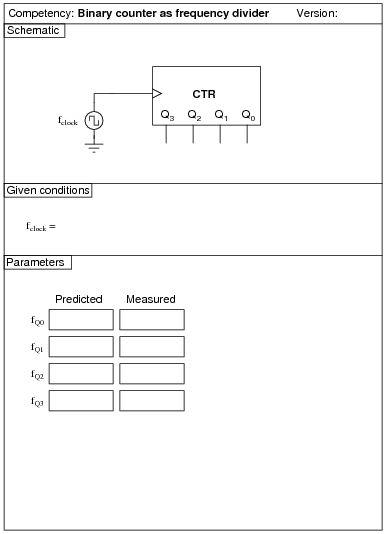
Question 36:
|
|
Notes:
Students are to research the datasheet for their particular IC and figure out from that what connections and timing sequences they need to make the circuit perform as requested. It is very important for students to learn to interpret manufacturers' datasheets!
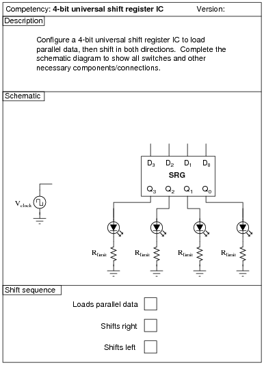
I recommend a slow clock frequency (1 Hz or so) to allow for easy viewing of the shift patterns. To conserve the number of necessary input switches, I allow students to hard-wire the data inputs (D0 through D3). This means they only need switches to control the mode of the shift register (parallel load, shift right, shift left, and shift inhibit).
Question 37:
|
|
Notes:
Students are to research the datasheet for their particular IC and figure out from that what connections and timing sequences they need to make the circuit perform as requested. It is very important for students to learn to interpret manufacturers' datasheets!
I recommend a slow clock frequency (1 Hz or so) to allow for easy viewing of the shift patterns. To conserve the number of necessary input switches, I allow students to hard-wire the data inputs (D0 through D3). This means they only need switches to control the mode of the shift register (parallel load, shift right, shift left, and shift inhibit).
Question 38:
|
|
Notes:
Use a four-pole, unipolar stepper motor for this assessment, with a power supply capable of sourcing the required current.
An extension of this exercise is to incorporate troubleshooting questions. Whether using this exercise as a performance assessment or simply as a concept-building lab, you might want to follow up your students' results by asking them to predict the consequences of certain circuit faults.
Question 39:
|
|
Notes:
An extension of this exercise is to incorporate troubleshooting questions. Whether using this exercise as a performance assessment or simply as a concept-building lab, you might want to follow up your students' results by asking them to predict the consequences of certain circuit faults.
Question 40:
|
|
Notes:
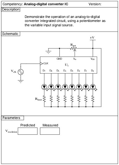
In this activity, students are asked to figure out the details of configuring the ADC: what power supply voltage to use, what resistor values, etc. The best source for this information is the ADC's datasheet!
For those students who have trouble figuring out how to calculate resolution, I recommend the following formula:
|
Where,
Vrange = "Span" of analog voltage input (how many volts of range it has from 00000000 to 11111111)
n = Number of output bits for the ADC
Question 41:
|
|
Notes:
Here, I let students choose appropriate values for Rpulldown and Rlimit, rather than specify them as given conditions.
Question 42:
|
|
Notes:
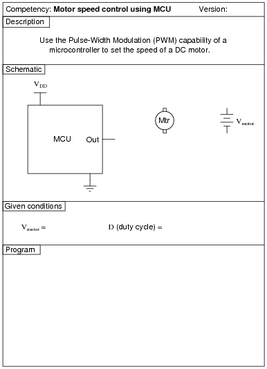
Here, I let students design and build their own transistor drive circuit to interpose between the MCU and the DC motor.
Question 43:
|
|
Notes:
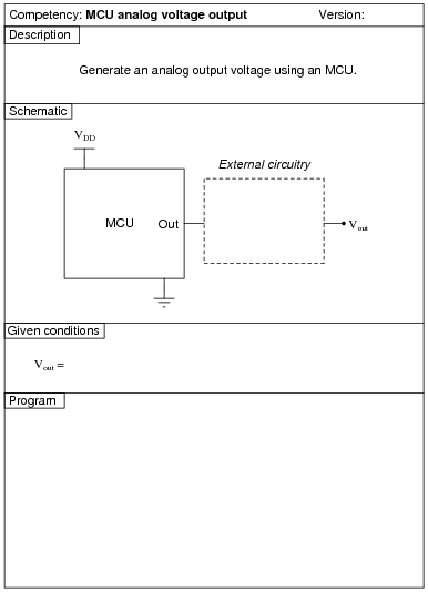
One method that is convenient for generating an analog output voltage with many microcontrollers is to program the MCU to generate a PWM output, then build an analog filter circuit to capture just the average DC value of that PWM waveform.