Binary math circuits
Question 1:
Add the following binary numbers:
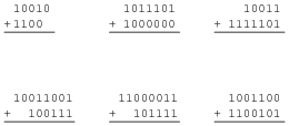
|
|
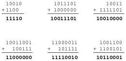
|
|
Notes:
Ask your students to describe what differences exist between manually adding binary numbers and manually adding decimal numbers, if any.
Question 2:
| Don't just sit there! Build something!! |
Learning to analyze digital circuits requires much study and practice. Typically, students practice by working through lots of sample problems and checking their answers against those provided by the textbook or the instructor. While this is good, there is a much better way.
You will learn much more by actually building and analyzing real circuits, letting your test equipment provide the änswers" instead of a book or another person. For successful circuit-building exercises, follow these steps:
- 1.
- Draw the schematic diagram for the digital circuit to be analyzed.
- 2.
- Carefully build this circuit on a breadboard or other convenient medium.
- 3.
- Check the accuracy of the circuit's construction, following each wire to each connection point, and verifying these elements one-by-one on the diagram.
- 4.
- Analyze the circuit, determining all output logic states for given input conditions.
- 5.
- Carefully measure those logic states, to verify the accuracy of your analysis.
- 6.
- If there are any errors, carefully check your circuit's construction against the diagram, then carefully re-analyze the circuit and re-measure.
Always be sure that the power supply voltage levels are within specification for the logic circuits you plan to use. If TTL, the power supply must be a 5-volt regulated supply, adjusted to a value as close to 5.0 volts DC as possible.
One way you can save time and reduce the possibility of error is to begin with a very simple circuit and incrementally add components to increase its complexity after each analysis, rather than building a whole new circuit for each practice problem. Another time-saving technique is to re-use the same components in a variety of different circuit configurations. This way, you won't have to measure any component's value more than once.
Notes:
It has been my experience that students require much practice with circuit analysis to become proficient. To this end, instructors usually provide their students with lots of practice problems to work through, and provide answers for students to check their work against. While this approach makes students proficient in circuit theory, it fails to fully educate them.
Students don't just need mathematical practice. They also need real, hands-on practice building circuits and using test equipment. So, I suggest the following alternative approach: students should build their own "practice problems" with real components, and try to predict the various logic states. This way, the digital theory "comes alive," and students gain practical proficiency they wouldn't gain merely by solving Boolean equations or simplifying Karnaugh maps.
Another reason for following this method of practice is to teach students scientific method: the process of testing a hypothesis (in this case, logic state predictions) by performing a real experiment. Students will also develop real troubleshooting skills as they occasionally make circuit construction errors.
Spend a few moments of time with your class to review some of the "rules" for building circuits before they begin. Discuss these issues with your students in the same Socratic manner you would normally discuss the worksheet questions, rather than simply telling them what they should and should not do. I never cease to be amazed at how poorly students grasp instructions when presented in a typical lecture (instructor monologue) format!
I highly recommend CMOS logic circuitry for at-home experiments, where students may not have access to a 5-volt regulated power supply. Modern CMOS circuitry is far more rugged with regard to static discharge than the first CMOS circuits, so fears of students harming these devices by not having a "proper" laboratory set up at home are largely unfounded.
A note to those instructors who may complain about the "wasted" time required to have students build real circuits instead of just mathematically analyzing theoretical circuits:
What is the purpose of students taking your course?
If your students will be working with real circuits, then they should learn on real circuits whenever possible. If your goal is to educate theoretical physicists, then stick with abstract analysis, by all means! But most of us plan for our students to do something in the real world with the education we give them. The "wasted" time spent building real circuits will pay huge dividends when it comes time for them to apply their knowledge to practical problems.
Furthermore, having students build their own practice problems teaches them how to perform primary research, thus empowering them to continue their electrical/electronics education autonomously.
In most sciences, realistic experiments are much more difficult and expensive to set up than electrical circuits. Nuclear physics, biology, geology, and chemistry professors would just love to be able to have their students apply advanced mathematics to real experiments posing no safety hazard and costing less than a textbook. They can't, but you can. Exploit the convenience inherent to your science, and get those students of yours practicing their math on lots of real circuits!
Question 3:
Identify each of these logic gates by name, and complete their respective truth tables:
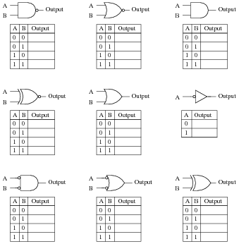
|
|
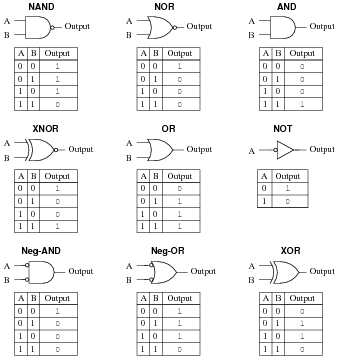
|
|
Notes:
In order to familiarize students with the standard logic gate types, I like to given them practice with identification and truth tables each day. Students need to be able to recognize these logic gate types at a glance, or else they will have difficulty analyzing circuits that use them.
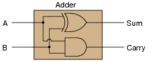
Question 4:
Design a circuit that adds two binary bits together. This circuit will have two inputs (A and B) and two outputs (Sum and Carry):
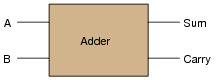
|
|
Begin the design process by drawing a truth table for the circuit, then determining the necessary gate circuitry to fulfill each output function.
Why is this circuit referred to as a half adder? How would a full adder circuit differ from this?
|
|
Notes:
Have your students explain their design process to you, step by step. This circuit diagram is easy enough to discover in the pages of a textbook, so don't be surprised if students simply copy what they see without trying to understand how it works!
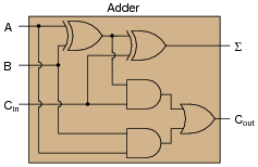
Question 5:
Design a circuit that adds two binary bits and a "Carry in" (Cin) bit together, producing a "Sum" (S) and a "Carry out" (Cout) output:
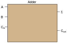
|
|
Begin the design process by drawing a truth table for the circuit, writing a boolean SOP expression for each output, then determining the necessary gate circuitry to fulfill each output function.
|
|
|
|
Notes:
Have your students explain their design process to you, step by step. This circuit diagram is easy enough to discover in the pages of a textbook, so don't be surprised if students simply copy what they see without trying to understand how it works!
Deriving the two cascaded Ex-OR gates from the boolean expression is a bit tricky, but not impossible. Remind your students if necessary that the boolean equivalent for the Ex-OR function is [`A]B + A[`B], and that the Ex-NOR function is AB +[`A] [`B].
Question 6:
Explain the difference between a ripple adder and a look-ahead adder. What does the term "ripple" mean in this context? Why is "ripple" potentially a bad thing for a digital adder circuit?
Notes:
The "ripple" effect seen in simple binary adder circuits is not limited to adders! Some Gray-to-binary code converters and counter circuits also exhibit ripple, with the same deleterious effects.
Question 7:
Compare the following two circuits, the first one being a digital adder and the second one being an analog summer:
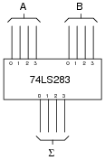
|
|
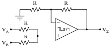
|
|
These two circuits perform the same mathematical function, yet the manners in which they perform this function are quite different. Compare and contrast the digital adder and the analog summer circuits shown here, citing any advantages or disadvantages of each.
- �
- Resolution
- �
- Accuracy
- �
- Speed
- �
- Cost
Notes:
This question is not really specific to adder/summer circuits, as it may first appear. The fundamental comparison being drawn in this question is between digital and analog. This is an important concept for students to grasp, as both have their roles in modern electronics. A common fallacy is that "digital is better" in all circumstances, but the truth is that both digital and analog have their respective strengths and limitations.
Question 8:
Explain the purpose of a magnitude comparator IC such as the 74LS85. What function, or functions, does it perform?
Notes:
Be sure to ask students where they obtained their information. It is very easy to obtain datasheets online (over the internet), making it convenient to assign short research projects such as this.
Question 9:
Research the datasheet of an integrated arithmetic logic unit such as the 74AS181, and determine how its various modes of operation (addition, subtraction, comparison) are selected.
Follow-up question: an interesting feature of the 74AS181 is that it provides ärithmetic" functions as well as "logic" functions. These two modes could also be referred to as "binary" and "boolean," respectively. Explain what distinguishes these two operating modes from one another, and why they are classified differently.
Notes:
Although the 74181 ALU is a somewhat dated IC (in fact, some versions are obsolete as of this writing - 2005), it stands as a simple example for students to learn from. A circuit such as this provides a good example of the power of integration, as opposed to constructing a similar logic function from individual gates (not to mention discrete transistors!).
The follow-up question brings up a point many students are confused on: the distinction between binary (numerical) and boolean (bitwise) operations. Binary is a place-weighted numeration system, used to symbolize real numbers using only two states per place. Boolean is a number system characterized by having only two possible values. Since both binary and boolean have something to do with two-valued quantities, many students believe the two to be interchangeable terms and concepts. However, they are not, and an investigation of the two operating modes of this ALU highlights the distinction.
Question 10:
An arithmetic trick often used when working with the metric system is multiplication-by-ten and division-by-ten via shifting of the decimal point. A similar "trick" may be applied to binary numbers, with similar results.
Determine what sort of multiplication or division is accomplished when the "binary point" is shifted in a binary number. Research the datasheet of an arithmetic logic unit (ALU) circuit to see if and how this function is implemented.
Challenge question: explain how multiplication or division by any binary quantity may be accomplished using successive bit-shifts and additions. For example, show what steps you could take to multiply any binary number by five (1012), using only "binary point" shifting and addition(s).
Notes:
A lot of arithmetic tricks existing in the decimal numeration system are applicable, with slight revision, in the binary numeration system as well. This is a popular one, and often used by shrewd computer programmers to execute fast multiply-by-two or divide-by-two operations when "conventional" multiplication commands take more time.
Question 11:
Explain the meaning of the digital lines A, B, F, and S in the following schematic diagram:
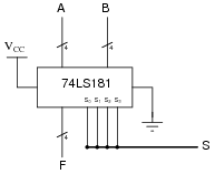
|
|
In case you were wondering, it is unusual to mix two different bus symbol conventions in the same schematic diagram. I show this here only for your benefit, to see that there is more than one ßtandard" way to draw it.
Notes:
The answer pretty much says it all. The fact that the IC is an ALU is quite incidental. Some students may research the part number to get a better understanding of what is going on. That is fine, but my emphasis in this question is the schematic diagram convention(s) for multi-conductor busses.