Class A BJT amplifiers
Question 1:
| Don't just sit there! Build something!! |
Learning to mathematically analyze circuits requires much study and practice. Typically, students practice by working through lots of sample problems and checking their answers against those provided by the textbook or the instructor. While this is good, there is a much better way.
You will learn much more by actually building and analyzing real circuits, letting your test equipment provide the änswers" instead of a book or another person. For successful circuit-building exercises, follow these steps:
- 1.
- Carefully measure and record all component values prior to circuit construction, choosing resistor values high enough to make damage to any active components unlikely.
- 2.
- Draw the schematic diagram for the circuit to be analyzed.
- 3.
- Carefully build this circuit on a breadboard or other convenient medium.
- 4.
- Check the accuracy of the circuit's construction, following each wire to each connection point, and verifying these elements one-by-one on the diagram.
- 5.
- Mathematically analyze the circuit, solving for all voltage and current values.
- 6.
- Carefully measure all voltages and currents, to verify the accuracy of your analysis.
- 7.
- If there are any substantial errors (greater than a few percent), carefully check your circuit's construction against the diagram, then carefully re-calculate the values and re-measure.
When students are first learning about semiconductor devices, and are most likely to damage them by making improper connections in their circuits, I recommend they experiment with large, high-wattage components (1N4001 rectifying diodes, TO-220 or TO-3 case power transistors, etc.), and using dry-cell battery power sources rather than a benchtop power supply. This decreases the likelihood of component damage.
As usual, avoid very high and very low resistor values, to avoid measurement errors caused by meter "loading" (on the high end) and to avoid transistor burnout (on the low end). I recommend resistors between 1 kW and 100 kW.
One way you can save time and reduce the possibility of error is to begin with a very simple circuit and incrementally add components to increase its complexity after each analysis, rather than building a whole new circuit for each practice problem. Another time-saving technique is to re-use the same components in a variety of different circuit configurations. This way, you won't have to measure any component's value more than once.
Notes:
It has been my experience that students require much practice with circuit analysis to become proficient. To this end, instructors usually provide their students with lots of practice problems to work through, and provide answers for students to check their work against. While this approach makes students proficient in circuit theory, it fails to fully educate them.
Students don't just need mathematical practice. They also need real, hands-on practice building circuits and using test equipment. So, I suggest the following alternative approach: students should build their own "practice problems" with real components, and try to mathematically predict the various voltage and current values. This way, the mathematical theory "comes alive," and students gain practical proficiency they wouldn't gain merely by solving equations.
Another reason for following this method of practice is to teach students scientific method: the process of testing a hypothesis (in this case, mathematical predictions) by performing a real experiment. Students will also develop real troubleshooting skills as they occasionally make circuit construction errors.
Spend a few moments of time with your class to review some of the "rules" for building circuits before they begin. Discuss these issues with your students in the same Socratic manner you would normally discuss the worksheet questions, rather than simply telling them what they should and should not do. I never cease to be amazed at how poorly students grasp instructions when presented in a typical lecture (instructor monologue) format!
A note to those instructors who may complain about the "wasted" time required to have students build real circuits instead of just mathematically analyzing theoretical circuits:
What is the purpose of students taking your course?
If your students will be working with real circuits, then they should learn on real circuits whenever possible. If your goal is to educate theoretical physicists, then stick with abstract analysis, by all means! But most of us plan for our students to do something in the real world with the education we give them. The "wasted" time spent building real circuits will pay huge dividends when it comes time for them to apply their knowledge to practical problems.
Furthermore, having students build their own practice problems teaches them how to perform primary research, thus empowering them to continue their electrical/electronics education autonomously.
In most sciences, realistic experiments are much more difficult and expensive to set up than electrical circuits. Nuclear physics, biology, geology, and chemistry professors would just love to be able to have their students apply advanced mathematics to real experiments posing no safety hazard and costing less than a textbook. They can't, but you can. Exploit the convenience inherent to your science, and get those students of yours practicing their math on lots of real circuits!
Question 2:
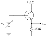
Complete the table of output voltages for several given values of input voltage in this common-collector amplifier circuit. Assume that the transistor is a standard silicon NPN unit, with a nominal base-emitter junction forward voltage of 0.7 volts:
|
|
-
Vin Vout
0.0 V
0.5 V
1.0 V
1.5 V
5.0 V
7.8 V
Based on the values you calculate, explain why the common-collector circuit configuration is often referred to as an emitter follower.
-
Vin Vout
0.0 V 0.0 V
0.5 V 0.0 V
1.0 V 0.3 V
1.5 V 0.8 V
5.0 V 4.3 V
7.8 V 7.1 V
The voltage at the transistor's emitter terminal approximately "follows" the voltage applied to the base terminal, hence the name.
Notes:
At first, the ëmitter follower" transistor circuit may seem pointless, since the output voltage practically equals the input voltage (especially for input voltages greatly exceeding 0.7 volts DC). "What possible good is a circuit like this?" some of your students may ask. The answer to this question, of course, has to do with currents in the circuit, and not necessarily voltages.
Question 3:
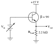
Complete the table of output voltages, output currents, and input currents for several given values of input voltage in this common-collector amplifier circuit. Assume that the transistor is a standard silicon NPN unit, with a nominal base-emitter junction forward voltage of 0.7 volts:
|
|
-
Vin Vout Iin Iout
0.0 V
0.4 V
1.2 V
3.4 V
7.1 V
10.8 V
Calculate the voltage and current gains of this circuit from the numerical values in the table:
|
|
-
Vin Vout Iin Iout
0.0 V 0.0 V 0.0 mA 0.0 mA
0.4 V 0.0 V 0.0 mA 0.0 mA
1.2 V 0.5 V 2.498 mA 0.227 mA
3.4 V 2.7 V 13.49 mA 1.227 mA
7.1 V 6.4 V 31.97 mA 2.909 mA
10.8 V 10.1 V 50.45 mA 4.591 mA
|
|
Notes:
The purpose of this question, besides providing practice for common-collector circuit DC analysis, is to show the current-amplification properties of the common-collector amplifier. This is an important feature, as there is no voltage amplification in this type of amplifier circuit.
This approach to determining transistor amplifier circuit voltage gain is one that does not require prior knowledge of amplifier configurations. In order to obtain the necessary data to calculate voltage gain, all one needs to know are the "first principles" of Ohm's Law, Kirchhoff's Laws, and basic operating principles of a bipolar junction transistor. This question is really just a thought experiment: exploring an unknown form of circuit by applying known rules of circuit components. If students doubt the efficacy of "thought experiments," one need only to reflect on the success of Albert Einstein, whose thought experiments as a patent clerk (without the aid of experimental equipment) allowed him to formulate the basis of his Theories of Relativity.
Question 4:
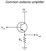
The following schematic diagram shows a simple common-collector transistor amplifier circuit:
|
|
Explain why the AC voltage gain (AV(AC)) of such an amplifier is approximately 1, using any or all of these general "rules" of transistor behavior:
- �
- IE = IC + IB
- �
- IE � IC
- �
- VBE � 0.7 volts
- �
- b = [(IC)/(IB)]
Remember that AC voltage gain is defined as [(DVout)/(DVin)].
For your discussion response, be prepared to explain why, in mathematical terms, the above statement is true. You will have to use Kirchhoff's Voltage Law as part of your explanation.
Notes:
Although the given answer seems complete, what I'm looking for here is a good analytical understanding of why the voltage gain is approximately 1. Placing the requirement of using KVL on the students' answers ensures that they will have to explore the concept further than the given answer does.
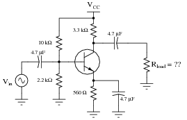
Question 5:
Calculate the approximate amount of AC voltage output by this common-collector amplifier circuit:
|
|
Also, explain why the reactance of each capacitor is a negligible factor in the operation of this amplifier circuit, assuming a signal frequency of 5 kHz.
Challenge question: calculate the approximate (average) DC voltage dropped across the 1 kW emitter resistor.
Notes:
Students should know the AC voltage gain of this amplifier configuration to be approximately 1, so the output voltage calculation should be trivial. This question is really a test to see whether or not students are able to apply their knowledge of voltage gain to a specific application.
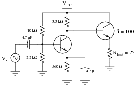
Question 6:
Calculate the approximate amount of AC voltage output by this common-collector amplifier circuit:
|
|
Also, determine a signal frequency value that yields less than 1 ohm of reactance for each of the two coupling capacitors.
Follow-up question: calculate the approximate (average) DC voltage dropped across the 1 kW emitter resistor.
Notes:
Students should know the AC voltage gain of this amplifier configuration to be approximately 1, so the output voltage calculation should be trivial. This question is really a test to see whether or not students are able to apply their knowledge of voltage gain to a specific application.
Question 7:
Calculate the approximate voltage gain (AV) for the following common-collector amplifier circuit, expressing it as a ratio and as a decibel value. Also calculate the quiescent DC voltage measured across the load resistor (Vload(DC)). Assume a silicon transistor:
|
|
- �
- AV (as a ratio) �
- �
- AV (in decibels) �
- �
- Vload(DC) �
- �
- AV (as a ratio) � 1
- �
- AV (in decibels) � 0 dB
- �
- Vload(DC) � 6.8 volts
Notes:
Nothing much to comment on here - just some practice on common-collector amplifier calculations. Note that the approximations given here are based on the following assumptions:
- �
- 0.7 volts drop (exactly) across base-emitter junction.
- �
- Infinite DC current gain (b) for transistor (IB = 0 mA ; IC = IE).
- �
- Negligible loading of bias voltage divider by the emitter resistance.
- �
- Negligible dynamic emitter resistance (r�e = 0 W )
This question lends itself well to group discussions on component failure scenarios. After discussing how to calculate the requested values, you might want to ask students to consider how these values would change given some specific component failures (open resistors, primarily, since this is perhaps the most common way that a resistor could fail).
Question 8:
Predict how all transistor currents (IB, IC, and IE) and the output voltage signal will be affected as a result of the following faults. Consider each fault independently (i.e. one at a time, no multiple faults):
|
|
- �
- Capacitor Cin fails open:
- �
- Solder bridge (short) past resistor R1:
- �
- Resistor R1 fails open:
- �
- Resistor RE fails open:
For each of these conditions, explain why the resulting effects will occur.
- �
- Capacitor Cin fails open: All transistor currents assume quiescent (DC) values, no output signal.
- �
- Solder bridge (short) past resistor R1: Transistor saturates (large increase in all currents), no output signal.
- �
- Resistor R1 fails open: All transistor currents fall to zero (transistor in complete cutoff mode), no output signal.
- �
- Resistor RE fails open: All transistor currents fall to zero (transistor in complete cutoff mode), no output signal.
Notes:
The purpose of this question is to approach the domain of circuit troubleshooting from a perspective of knowing what the fault is, rather than only knowing what the symptoms are. Although this is not necessarily a realistic perspective, it helps students build the foundational knowledge necessary to diagnose a faulted circuit from empirical data. Questions such as this should be followed (eventually) by other questions asking students to identify likely faults based on measurements.
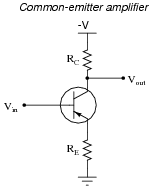
Question 9:
Complete the table of voltages and currents for several given values of input voltage in this common-emitter amplifier circuit. Assume that the transistor is a standard silicon NPN unit, with a nominal base-emitter junction forward voltage of 0.7 volts. For the last row of the table, give qualitative answers (increase, decrease, or same) representing what each of the quantities will do given an increasing base voltage (VB):
|
|
-
VB VE IC VRC VCE VC (Vout)
0.0 V
0.5 V
1.0 V
1.5 V
2.0 V
2.5 V
3.0 V
increase
Calculate the voltage gain of this circuit from the numerical values in the table:
|
-
VB VE IC VRC VCE VC (Vout)
0.0 V 0.0 V 0.0 mA 0.0 V 15 V 15 V
0.5 V 0.0 V 0.0 mA 0.0 V 15 V 15 V
1.0 V 0.3 V 0.298 mA 1.40 V 13.3 V 13.6 V
1.5 V 0.8 V 0.793 mA 3.73 V 10.47 V 11.27 V
2.0 V 1.3 V 1.29 mA 6.06 V 7.64 V 8.94 V
2.5 V 1.8 V 1.79 mA 8.39 V 4.81 V 6.61 V
3.0 V 2.3 V 2.28 mA 10.7 V 1.98 V 4.28 V
increase increase increase increase decrease decrease
|
Sometimes the voltage gain of a common-emitter amplifier circuit is expressed as a negative quantity (-4.66 in this case), to indicate the inverse output/input relationship (180o phase shift).
Follow-up question: what similarity do you notice between the voltage gain value of 4.66 and the two resistor values?
Challenge question: a common assumption used in this type of BJT amplifier circuit is IC � IE. Develop a voltage gain formula based on this assumption, in terms of resistor values RC and RE.
Notes:
The purpose of this question, besides providing practice for common-emitter circuit DC analysis, is to show the signal-inverting and voltage-amplification properties of the common-emitter amplifier. Some students experience difficulty understanding why VC (the output voltage) decreases with increasing base voltage (VB). Working through the numbers in this table gives concrete proof why it is so.
This approach to determining transistor amplifier circuit voltage gain is one that does not require prior knowledge of amplifier configurations. In order to obtain the necessary data to calculate voltage gain, all one needs to know are the "first principles" of Ohm's Law, Kirchhoff's Laws, and basic operating principles of a bipolar junction transistor. This question is really just a thought experiment: exploring an unknown form of circuit by applying known rules of circuit components. If students doubt the efficacy of "thought experiments," one need only to reflect on the success of Albert Einstein, whose thought experiments as a patent clerk (without the aid of experimental equipment) allowed him to formulate the basis of his Theories of Relativity.
Question 10:
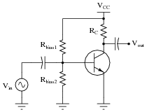
The following schematic diagram shows a simple common-emitter transistor amplifier circuit:
|
|
Explain why the voltage gain (AV) of such an amplifier is approximately [(RC)/(RE)], using any or all of these general "rules" of transistor behavior:
- �
- IE = IC + IB
- �
- IE � IC
- �
- VBE � 0.7 volts
- �
- b = [(IC)/(IB)]
Remember that (AC) voltage gain is defined as [(DVout)/(DVin)]. Hint: this question might be easier to answer if you first consider how to explain the unity-gain of a common-collector amplifier circuit (simply eliminate RC, replacing it with a direct connection to -V, and consider VE to be the output voltage).
For your discussion response, be prepared to explain everything in mathematical terms. You will have to use Kirchhoff's Voltage Law at least once to be able to do this completely.
Notes:
Although the given answer seems complete, what I'm looking for here is a good analytical understanding of why the voltage gain is what it is. Placing the requirement of using KVL on the students' answers ensures that they will have to explore the concept further than the given answer does.
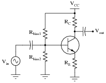
Question 11:
Determine what would happen to the voltage gain of a common-emitter transistor amplifier circuit if the following resistance values were changed (consider one change at a time):

|
|
- �
- Resistance RC increased; AV . . .
- �
- Resistance RE increased; AV . . .
- �
- Resistance Rbias1 increased; AV . . .
- �
- Resistance Rbias2 increased; AV . . .
- �
- Resistance RC increased; AV increases
- �
- Resistance RE increased; AV decreases
- �
- Resistance Rbias1 increased; AV does not change
- �
- Resistance Rbias2 increased; AV does not change
Notes:
The purpose of this question is to get students to apply their knowledge of common-emitter amplifier voltage gain to hypothetical changes in resistance. These are important concepts, so be sure to discuss them adequately, challenging your students to explain why the voltage gain is affected as described, not just explained by blindly following a gain formula.
Many students experience difficulty understanding why voltage gain is directly proportional to collector resistance. What they visualize when they consider a greater collector resistance is less collector voltage, which they understandably equate to less output signal and thus less gain. While the quiescent (DC) output voltage does decrease with increasing RC, what is not so obvious is that change in collector voltage (DVC) increases with increasing RC.
Ask your students to explain why changes in bias resistor values do not (significantly) effect voltage gain. Does this mean the values are arbitrary? Discuss with them the purpose of bias resistors, if necessary, and what would happen if they were not there or if they were grossly mis-sized.
Question 12:
A student attempts to calculate the voltage gain of the following common-emitter amplifier circuit, and arrives at an incalculable value (divide-by-zero error):
|
|
According to a simple formula for approximating the voltage gain of this type of amplifier, it would indeed seem as though this circuit would have infinite voltage gain with zero emitter resistance. However, even with no emitter resistor installed in such a circuit, the transistor itself contains a small amount of resistance intrinsic to the semiconductor material, commonly symbolized as r�e:

|
|
The problem is, this resistance value r�e is far from stable. Determine some of the factors influencing the value of the transistor's intrinsic emitter resistance, and explain why a circuit such as the one first shown in this question would be very unstable (possibly resulting in the self-destruction of the transistor!).
|
Follow-up question: explain why this dynamic emitter resistance is often ignored when calculating voltage gain in a common-emitter circuit such as this:
|
|
Notes:
This question may serve as a good starting point for a discussion on thermal runaway, discussing how r�e decreases with temperature, increasing IE, once again decreasing r�e, an infinitum, ad destructum.
The follow-up question provides a good opportunity to discuss the engineering principle of swamping: when two quantities are unequal to the extent that one renders the other relatively insignificant. This concept is very important in analysis because it allows us to construct simpler models of realistic processes than we could if we had to take every factor into account. It is also important in design because it allows us to overshadow certain unwanted effects.
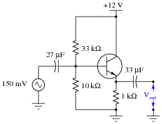
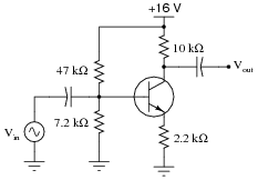
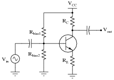
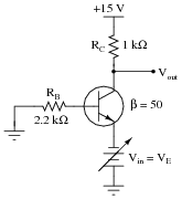
Question 13:
Calculate the approximate voltage gain (AV) for the following common-emitter amplifier circuit, and also calculate the quiescent DC voltages measured at the three terminals of the transistor with respect to ground (VB, VE, and VC). Assume a silicon transistor:
|
|
- �
- AV �
- �
- VB �
- �
- VE �
- �
- VC �
- �
- AV � 4.55
- �
- VB � 2.125 volts
- �
- VE � 1.425 volts
- �
- VC � 9.521 volts
Notes:
Nothing much to comment on here - just some practice on common-emitter amplifier calculations. Note that the approximations given here are based on the following assumptions:
- �
- 0.7 volts drop (exactly) across base-emitter junction.
- �
- Infinite DC current gain (b) for transistor (IB = 0 mA ; IC = IE).
- �
- Negligible loading of bias voltage divider by the emitter resistance.
- �
- Negligible dynamic emitter resistance (r�e = 0 W )
This question lends itself well to group discussions on component failure scenarios. After discussing how to calculate the requested values, you might want to ask students to consider how these values would change given some specific component failures (open resistors, primarily, since this is perhaps the most common way that a resistor could fail).
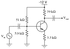
Question 14:
Calculate the approximate voltage gain (AV) for the following common-emitter amplifier circuit, and also calculate the quiescent DC voltages measured at the three terminals of the transistor with respect to ground (VB, VE, and VC). Assume a silicon transistor:
|
|
- �
- AV �
- �
- VB �
- �
- VE �
- �
- VC �
- �
- AV � 7.02
- �
- VB � 2.273 volts
- �
- VE � 1.573 volts
- �
- VC � 13.96 volts
Notes:
Nothing much to comment on here - just some practice on common-emitter amplifier calculations. Note that the approximations given here are based on the following assumptions:
- �
- 0.7 volts drop (exactly) across base-emitter junction.
- �
- Infinite DC current gain (b) for transistor (IB = 0 mA ; IC = IE).
- �
- Negligible loading of bias voltage divider by the emitter resistance.
- �
- Negligible dynamic emitter resistance (r�e = 0 W )
This question lends itself well to group discussions on component failure scenarios. After discussing how to calculate the requested values, you might want to ask students to consider how these values would change given some specific component failures (open resistors, primarily, since this is perhaps the most common way that a resistor could fail).
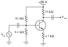
Question 15:
Calculate the approximate voltage gain (AV) for the following common-emitter amplifier circuit, and also calculate the quiescent DC voltages measured at the three terminals of the transistor with respect to ground (VB, VE, and VC). Assume a silicon transistor:
|
|
- �
- AV �
- �
- VB �
- �
- VE �
- �
- VC �
- �
- AV � 11.8
- �
- VB � -1.244 volts
- �
- VE � -0.544 volts
- �
- VC � -5.568 volts
Notes:
Nothing much to comment on here - just some practice on common-emitter amplifier calculations. Note that the approximations given here are based on the following assumptions:
- �
- 0.7 volts drop (exactly) across base-emitter junction.
- �
- Infinite DC current gain (b) for transistor (IB = 0 mA ; IC = IE).
- �
- Negligible loading of bias voltage divider by the emitter resistance.
- �
- Negligible dynamic emitter resistance (r�e = 0 W )
This question lends itself well to group discussions on component failure scenarios. After discussing how to calculate the requested values, you might want to ask students to consider how these values would change given some specific component failures (open resistors, primarily, since this is perhaps the most common way that a resistor could fail).
Question 16:
Choose values for the collector and emitter resistors that will yield a voltage gain of approximately 5 for the following common-emitter amplifier circuit:
|
|
- �
- RC =
- �
- RE =
- �
- RC = 10 kW
- �
- RE = 2 kW
Notes:
You might want to ask your students what practical maximum and minimum resistor values they would choose between when designing such an amplifier circuit. What would be the danger of selecting resistors too low in value? What would be wrong with choosing resistors too high in value? They might not be ready to answer these questions (especially the latter) until after having studied amplifier impedance calculations, though!
Question 17:
Calculate the approximate voltage gain (AV) for the following bypassed common-emitter amplifier circuit, assuming a quiescent (DC) emitter current value of 750 mA. Also calculate the quiescent DC voltage measured at the transistor's collector terminal with respect to ground (VC). Assume a silicon transistor:
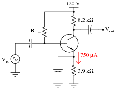
|
|
- �
- AV �
- �
- VC �
- �
- AV � 246
- �
- VC � 13.85 volts
Notes:
Nothing much to comment on here - just some practice on common-emitter amplifier calculations. Note that the approximations given here are based on the following assumptions:
- �
- 0.7 volts drop (exactly) across base-emitter junction.
- �
- Infinite DC current gain (b) for transistor (IB = 0 mA ; IC = IE).
- �
- Negligible loading of bias voltage divider by the emitter resistance.
- �
- Negligible dynamic emitter resistance (r�e = 0 W )
This question lends itself well to group discussions on component failure scenarios. After discussing how to calculate the requested values, you might want to ask students to consider how these values would change given some specific component failures (open resistors, primarily, since this is perhaps the most common way that a resistor could fail).
Question 18:
Calculate the approximate voltage gain (AV) for the following common-emitter amplifier circuit, expressing it both as a ratio and as a figure in decibels. Also calculate the quiescent DC voltages measured at the three terminals of the transistor with respect to ground (VB, VE, and VC). Assume a silicon transistor:

|
|
- �
- AV (as a ratio) �
- �
- AV (in decibels) �
- �
- VB �
- �
- VE �
- �
- VC �
- �
- AV (as a ratio) � 8.148
- �
- AV (in decibels) � 18.22 dB
- �
- VB � -1.355 volts
- �
- VE � -0.655 volts
- �
- VC � -6.664 volts
Notes:
Nothing much to comment on here - just some practice on common-emitter amplifier calculations. Note that the approximations given here are based on the following assumptions:
- �
- 0.7 volts drop (exactly) across base-emitter junction.
- �
- Infinite DC current gain (b) for transistor (IB = 0 mA ; IC = IE).
- �
- Negligible loading of bias voltage divider by the emitter resistance.
- �
- Negligible dynamic emitter resistance (r�e = 0 W )
This question lends itself well to group discussions on component failure scenarios. After discussing how to calculate the requested values, you might want to ask students to consider how these values would change given some specific component failures (open resistors, primarily, since this is perhaps the most common way that a resistor could fail).
Question 19:
Predict how all transistor currents (IB, IC, and IE) and the output voltage signal will be affected as a result of the following faults. Consider each fault independently (i.e. one at a time, no multiple faults):
|
|
- �
- Capacitor Cin fails open:
- �
- Solder bridge (short) past resistor R1:
- �
- Resistor R1 fails open:
- �
- Resistor RC fails open:
- �
- Resistor RE fails open:
- �
- Capacitor Cbypass fails shorted:
For each of these conditions, explain why the resulting effects will occur.
- �
- Capacitor Cin fails open: All transistor currents assume quiescent (DC) values, no output signal.
- �
- Solder bridge (short) past resistor R1: Transistor saturates (large increase in all currents), no output signal.
- �
- Resistor R1 fails open: All transistor currents fall to zero (transistor in complete cutoff mode), no output signal.
- �
- Resistor RC fails open: Transistor base current will decrease, zero collector current, greatly decreased emitter current, no output signal.
- �
- Resistor RE fails open: All transistor currents fall to zero (transistor in complete cutoff mode), no output signal.
- �
- Capacitor Cbypass fails shorted: Transistor saturates (large increase in all currents), no output signal.
Notes:
The purpose of this question is to approach the domain of circuit troubleshooting from a perspective of knowing what the fault is, rather than only knowing what the symptoms are. Although this is not necessarily a realistic perspective, it helps students build the foundational knowledge necessary to diagnose a faulted circuit from empirical data. Questions such as this should be followed (eventually) by other questions asking students to identify likely faults based on measurements.
Question 20:
Complete the table of voltages and currents for several given values of input voltage in this common-base amplifier circuit. Assume that the transistor is a standard silicon NPN unit, with a nominal base-base junction forward voltage of 0.7 volts:
|
|
-
VE VB IB IC VRC VC
0.0 V
-0.5 V
-0.8 V
-1.0 V
-1.1 V
-1.2 V
-1.3 V
Calculate the voltage gain of this circuit from the numerical values in the table:
|
-
VE VB IB IC VRC VC
0.0 V 0.0 V 0.0 mA 0.0 mA 0.0 V 15 V
-0.5 V 0.0 V 0.0 mA 0.0 mA 0.0 V 15 V
-0.8 V -0.1 V 45.5 mA 2.27 mA 2.27 V 12.7 V
-1.0 V -0.3 V 136.4 mA 6.82 mA 6.82 V 8.18 V
-1.1 V -0.4 V 181.8 mA 9.09 mA 9.09 V 5.91 V
-1.2 V -0.5 V 227.3 mA 11.36 mA 11.36 V 3.64 V
-1.3 V -0.6 V 272.7 mA 13.64 mA 13.64 V 1.36 V
|
Follow-up question: based on the values for output and input voltage shown in the table, would you say that common-base amplifier circuits are inverting or noninverting?
Notes:
The purpose of this question, besides providing practice for common-base circuit DC analysis, is to show the noninverting and voltage-amplification properties of the common-base amplifier, as well as to showcase its low current gain.
The negative values shown for emitter voltage (Vin) are correct and intentional. It is necessary to view the input voltage as a negative quantity to confidently determine the phase relationship between input and output.
This approach to determining transistor amplifier circuit voltage gain is one that does not require prior knowledge of amplifier configurations. In order to obtain the necessary data to calculate voltage gain, all one needs to know are the "first principles" of Ohm's Law, Kirchhoff's Laws, and basic operating principles of a bipolar junction transistor. This question is really just a thought experiment: exploring an unknown form of circuit by applying known rules of circuit components. If students doubt the efficacy of "thought experiments," one need only to reflect on the success of Albert Einstein, whose thought experiments as a patent clerk (without the aid of experimental equipment) allowed him to formulate the basis of his Theories of Relativity.
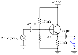
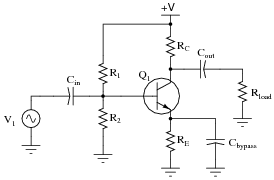
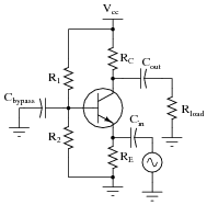
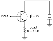
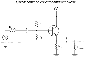
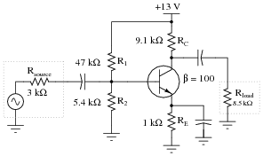
Question 21:
Describe the functions of resistors R1 and R2, and capacitor C1, in this amplifier circuit. What purpose do they serve?
|
|
Would it be possible for this amplifier circuit to operate in Class A mode without this voltage divider/capacitor network? Explain your answer.
While other biasing networks are possible for a Class A amplifier circuit, some type of DC bias voltage is necessary to make a bipolar junction transistor operate in Class A mode.
Notes:
Discuss with your students the meaning of "Class A" amplification, and why DC biasing is necessary in order to achieve this mode of operation in a BJT circuit.
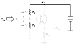
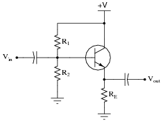
Question 22:
Explain the effects of increasing R3's resistance in this amplifier circuit. As R3 becomes more resistive, will the input signal (Vin) have more or less effect on the output voltage (Vout) than before? Express your answer in terms of voltage gain (AV).
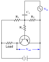
|
|
Notes:
While the answer to this question will be obvious to some, it will not be obvious to all. Ask those students who do understand the answer to explain - using their own words - why the voltage gain decreases as R3's resistance increases.
Ask your students to imagine two scenarios of extreme resistance change for R3: shorted and open. Qualitative analysis of the circuit should be rather easy given these extreme conditions! Then, ask your students to relate the results of these hypothetical scenarios with a simple increase in resistance. Is there a general problem-solving technique at work here? Challenge your students to explain how this technique works.
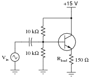
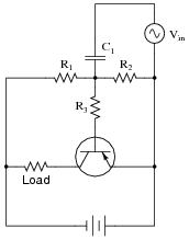
Question 23:
Explain the effects of increasing the load resistance in this amplifier circuit. As the load becomes more resistive, will the input signal (Vin) have more or less effect on the output voltage (Vout) than before? Express your answer in terms of voltage gain (AV).

|
|
Notes:
Ask your students to imagine two scenarios of extreme resistance change for R3: shorted and open. Does this "thought experiment" help to see the effects of changing load resistance? If not, imagine two (lesser) extreme load resistance values: 1 ohm versus 1 million ohms. Now is the effect of load resistance change apparent?
Another question to provoke deep thought about this circuit is to ask what the effects of load resistance change will be on this circuit's load line. Does a greater load resistance make for a steeper load line, or a shallower load line? How does this relate to voltage gain?
Question 24:
Explain how you could measure the AC voltage gain of a functioning Class A amplifier circuit, as opposed to predicting its gain from known component values.
|
Notes:
This skill is important if students are to build amplifier circuits and empirically compare their performance against predicted results.
Question 25:
Identify the type of transistor amplifier configuration in these schematic diagrams as either common-emitter, common-collector, or common-base.
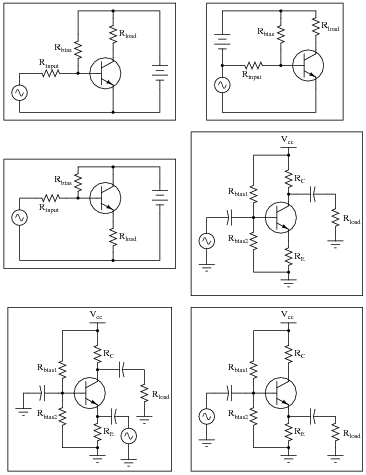
|
|
|
|
Notes:
I have seen more than one method for determining the "common-ness" of an amplifier configuration, and not all are satisfying. Rather than telling your students how to distinguish one amplifier type from the others, let them examine the different configurations in the answer and figure out their own method(s)!
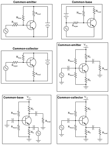
Question 26:
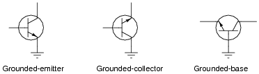
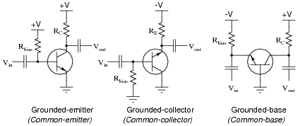
Common-emitter, common-collector, and common-base amplifier circuits are sometimes referred to as grounded-emitter, grounded-collector, and grounded-base, respectively, because these configurations may actually be built with those respective terminals connected straight to ground.
Although this may not be very practical for ease of biasing, it can be done. Draw the rest of the circuit necessary to provide class-A operation for each of these (partial) transistor circuits. Be sure to show where the DC power source, signal input, and signal output connect:
|
|
|
|
Notes:
Although it is more common in modern times to refer to the three BJT amplifier configurations as common-(e, c, b) rather than as grounded-(e, c, b), it may help some students grasp why the word "common" came to be used. "Grounded" makes more literal sense, and seeing these three circuit configurations with directly grounded terminals may serve as a starting point for identifying configurations where the "common" terminals are not directly grounded.
Question 27:
Define what a common-collector transistor amplifier circuit is. What distinguishes this amplifier configuration from the other single-BJT amplifier configurations, namely common-emitter and common-base?
Also, describe the typical gains (voltage and current) of this amplifier configuration, and whether it is inverting or noninverting.
Common-collector amplifiers are characterized by high current gains, voltage gains of 1 or (slightly) less, and a noninverting phase relationship between input and output.
Notes:
The answers to the question may be easily found in any fundamental electronics text, but it is important to ensure students know why these characteristics are such. I always like to tell my students, "Memory will fail you, so you need to build an understanding of why things are, not just what things are."
Question 28:
Define what a common-emitter transistor amplifier circuit is. What distinguishes this amplifier configuration from the other single-BJT amplifier configurations, namely common-collector and common-base?
Also, describe the typical gains (voltage and current) of this amplifier configuration, and whether it is inverting or noninverting.
Common-emitter amplifiers are characterized by moderate voltage and current gains, and an inverting phase relationship between input and output.
Notes:
The answers to the question may be easily found in any fundamental electronics text, but it is important to ensure students know why these characteristics are such. I always like to tell my students, "Memory will fail you, so you need to build an understanding of why things are, not just what things are."
One exercise you might have your students do is come up to the board in front of the room and draw an example of this circuit, then everyone may refer to the drawn image when discussing the circuit's characteristics.
Question 29:
Define what a common-base transistor amplifier circuit is. What distinguishes this amplifier configuration from the other single-BJT amplifier configurations, namely common-collector and common-emitter?
Also, describe the typical gains (voltage and current) of this amplifier configuration, and whether it is inverting or noninverting.
Common-base amplifiers are characterized by high voltage gains, current gains less than unity, and a noninverting phase relationship between input and output.
Notes:
The answers to the question may be easily found in any fundamental electronics text, but it is important to ensure students know why these characteristics are such. I always like to tell my students, "Memory will fail you, so you need to build an understanding of why things are, not just what things are."
One exercise you might have your students do is come up to the board in front of the room and draw an example of this circuit, then everyone may refer to the drawn image when discussing the circuit's characteristics.
Question 30:
Compared to common-collector and common-emitter amplifiers, common-base circuits have few practical applications. Explain why.
Notes:
Perhaps the most frequent application of the common-base amplifier topology is the so-called cascode amplifier circuit, where a common-emitter stage acts as a "front-end" buffer to the common-base stage to provide reasonable input impedance and current gain. The grounded-base configuration of the final output stage virtually eliminates the undesirable effects of Miller (collector-to-base) capacitance, resulting in an amplifier capable of high-frequency operation with little or no neutralization required.
Question 31:
Predict how all transistor currents (IB, IC, and IE) and the output voltage signal will be affected as a result of the following faults. Consider each fault independently (i.e. one at a time, no multiple faults):
|
|
- �
- Capacitor Cout fails open:
- �
- Solder bridge (short) past resistor R1:
- �
- Resistor R1 fails open:
- �
- Resistor RC fails open:
- �
- Resistor RE fails open:
- �
- Capacitor Cbypass fails shorted:
For each of these conditions, explain why the resulting effects will occur.
- �
- Capacitor Cout fails open: Transistor currents unaffected, no output signal.
- �
- Solder bridge (short) past resistor R1: Transistor saturates (large increase in all currents), no output signal.
- �
- Resistor R1 fails open: All transistor currents fall to zero (transistor in complete cutoff mode), no output signal.
- �
- Resistor RC fails open: Transistor base current will decrease, zero collector current, greatly decreased emitter current, no output signal.
- �
- Resistor RE fails open: All transistor currents fall to zero (transistor in complete cutoff mode), no output signal.
- �
- Capacitor Cbypass fails shorted: All transistor currents fall to zero (transistor in complete cutoff mode), no output signal.
Notes:
The purpose of this question is to approach the domain of circuit troubleshooting from a perspective of knowing what the fault is, rather than only knowing what the symptoms are. Although this is not necessarily a realistic perspective, it helps students build the foundational knowledge necessary to diagnose a faulted circuit from empirical data. Questions such as this should be followed (eventually) by other questions asking students to identify likely faults based on measurements.
Question 32:
The voltage gain of this amplifier circuit, unlike other amplifier configurations, is completely independent of the load resistor value:
|
|
No matter what the resistance of the load, the amplifier's voltage gain remains the same. Explain why this is so.
Notes:
I have found it helpful to approach this amplifier circuit from the perspective of a constant DC input voltage, qualitatively analyzing the voltage across the load resistor as it increases from a power-up condition. Students will see that the transistor goes into cutoff mode if the load voltage ever exceeds the total DC input voltage at the transistor's base terminal, and will saturate if the load voltage ever falls below Vin - 0.7 volts.
Question 33:
Temperature changes are well known to affect transistor operation. For instance, if we were to apply a constant voltage between the base and emitter of a transistor and increase its temperature over time, the collector current would increase:
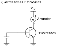
|
|
First, describe why the collector current changes, if the input voltage is held constant. Then, determine the relative degree of output voltage change (DVout) resulting from this thermal effect in the following two amplifier circuits:
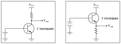
|
|
What is different in the responses of these two circuits to temperature changes? Why does one circuit respond so much differently than the other?
If both these amplifier circuits had AC signal inputs, and were biased for Class A operation, what effect would an increase in temperature have on each of them? State your answer in terms of AC voltage gain and Q-point.
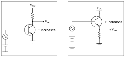
|
|
In the common-emitter amplifier circuit, the output voltage will change substantially with changes in transistor temperature. In the common-collector circuit, the output voltage will hardly change at all as transistor temperature changes.
When amplifying AC input signals, the common-emitter amplifier's voltage gain will increase, while the common-collector amplifier's voltage gain will remain at unity. Likewise, the common-emitter amplifier's Q point will shift substantially, while the common-collector amplifier's Q point will not.
Notes:
Discuss the impact of emitter resistance change on base current, and then transfer this concept to the two amplifier circuits and note the effects. Students should immediately realize the effects of this change in the common-emitter circuit, but the effects in the common-collector circuit will be a bit more difficult to follow. Work with your students in the analysis of the common-collector circuit, noting the effect changes in load voltage (voltage across the resistor) have on base current.
This question also previews the concept of negative feedback, which will be essential to your students' understanding of electronic circuits later in their studies.
Question 34:
One major different between a common-emitter amplifier configuration and a common-collector amplifier configuration is a principle called negative feedback, where changes in output voltage "feed back" to influence the amplifier's input signal, which in turn influences the output voltage again. Common-collector amplifier circuits have large amounts of negative feedback inherent to their design.
The absence or presence of negative feedback in an amplifier circuit has profound effects on voltage gain (AV). Compare the relative voltage gains of the following amplifiers:
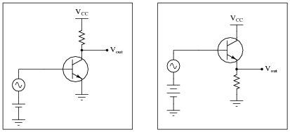
|
|
At first, the low voltage gain of the common-collector amplifier may appear to be a disadvantage of that circuit design. However, there is one major benefit relevant to the common-collector amplifier's voltage gain, being a direct result of negative feedback. What is this advantage?
Notes:
Discuss with your students the many factors that can influence voltage gain in a common-emitter amplifier circuit, and then compare that relative instability with the rock-solid stability of the common-collector amplifier's voltage gain. What benefit is it to a circuit designer to have a stable voltage gain from a particular amplifier design?
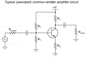
Question 35:
One way to reap the advantages of negative feedback enjoyed in common-collector amplifier circuits, in a common-emitter amplifier, is to add components that intentionally "feed back" some of the output signal to the transistor's input in a degenerative fashion:
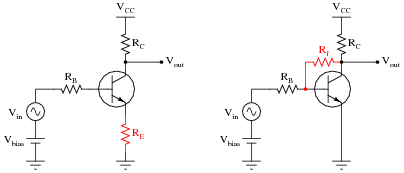
|
|
Explain what the term negative (or degenerative) means with reference to feedback, and explain how each of these techniques works to produce this type of feedback. Also, explain one disadvantage of applying negative feedback to a common-emitter amplifier circuit.
The use of an emitter resistor (RE) simply makes the amplifier circuit look more like a common-collector configuration, and the feedback functions in the same way. The use of a "feedback" resistor (Rf) takes advantage of the common-emitter's inverting nature, the output signal being 180o out of phase with the input.
Applying negative feedback to a common-emitter amplifier has the effect of decreasing its voltage gain.
Notes:
Negative feedback is a vitally important principle for electronics students to understand. It is the basis of almost every type of control system, and it makes standardized amplifier design possible. Take as much time as necessary to discuss this with your students, and to make sure they understand how and why negative feedback works as it does.
Be sure to discuss the twin effects of negative feedback: increased voltage gain stability, and decreased voltage gain. Ask your students why anyone would want their amplifier circuit to suffer a loss of voltage gain just for the sake of gain stability. Why is the stability if voltage gain important?
Question 36:
Sometimes a feedback network is purposely placed in an amplifier circuit, like the Rf-Cf combination shown in the following schematic:
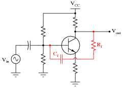
|
|
Explain what will happen to the amplifier circuit's performance if either one of the components in this feedback network fails open.
Notes:
The purpose of this question is to approach the domain of circuit troubleshooting from a perspective of knowing what the fault is, rather than only knowing what the symptoms are. Although this is not necessarily a realistic perspective, it helps students build the foundational knowledge necessary to diagnose a faulted circuit from empirical data. Questions such as this should be followed (eventually) by other questions asking students to identify likely faults based on measurements.
Question 37:
Amplifier distortion occurs when its gain varies as a function of the instantaneous signal amplitude. That is, some parts of the signal waveform become amplified more than others, and this results in the waveform taking on a slightly different shape.
All active devices, bipolar junction transistors included, are nonlinear to some extent. This term means that their gain varies throughout their operating ranges. During the 1920's, an electrical engineer named Harold Black was pondering this problem in the design of telephone system amplifiers. His solution came to him in a flash of insight one day, as he was commuting from work on a ferry boat. Explain what his solution to this problem was.
Challenge question: since negative feedback has the undesirable effect of diminishing overall amplifier gain, it would seem at first that low distortion and high gain are mutually exclusive design goals for an amplifier. Is this true, or is there a way to obtain both low distortion and high gain from an amplifier? If so, how?
Notes:
Although Black's solution has been wildly successful in amplifier design, it also finds application in a wide range of processes. Control theory, for example, where machines are automated in such a way as to stabilize physical variables such as pressure, flow, temperature, etc., depends heavily on negative feedback as an operating principle.
An interesting historical side-note is that Black's 1928 patent application was initially rejected on the grounds that he was trying to submit a perpetual motion device! The concept of negative feedback in an amplifier circuit was so contrary to established engineering thought at the time, that Black experienced significant resistance to the idea within the engineering community. At that time the United States patent office was inundated with fraudulent "perpetual motion" claims, and so dismissed Black's invention at first sight.
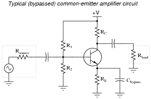
Question 38:
A popular method of "reclaiming" some of the lost voltage gain resulting from the addition of an emitter resistor (RE) to a common-emitter amplifier circuit is to connect a "bypass" capacitor in parallel with that resistor:
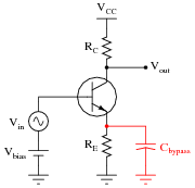
|
|
Explain why this technique works to increase the circuit's AC voltage gain, without leading to the problems associated with directly grounding the emitter.
The addition of a bypass capacitor maintains DC stability, because DC cannot go through the capacitor but must go through the emitter resistor (RE) just as if the bypass capacitor were not there at all.
Notes:
This question provides a good opportunity to review capacitive reactance (XC). The polarized capacitor symbol hints at the capacitor's relatively large value, and your students should realize that a large capacitor's reactance will be relatively low to most AC signals. An idea to help communicate the "bypass" concept is to have one of your students re-draw the circuit as ßeen" from the perspective of an AC signal, not a DC signal. With the capacitor effectively acting as a short-circuit to AC signals, what does the amplifier circuit look like to those signals?
Question 39:
Some common-emitter amplifier circuits use partial bypassing of emitter resistance, with the bypass capacitor connected in parallel with only one of two series resistors:
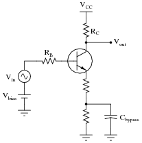
|
|
Explain the purpose of this arrangement. How does this differ in performance from the simple one-resistor emitter feedback design, or a grounded-emitter amplifier with no emitter resistor at all?
Notes:
After reviewing the simple (no-resistor) common-emitter circuit design, and the full-bypass design, it should be apparent to students that this circuit is a hybrid of the two previous designs. Likewise, it should come as little surprise that its performance characteristics lie somewhere between the two previous designs.
Question 40:
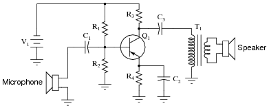
A student builds this common-emitter amplifier so they he may amplify the audio signals from a microphone to power a speaker:
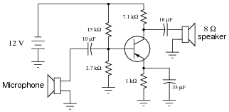
|
|
Unfortunately, the results are considerably less than expected: although some sound does come out of the speaker, it is not enough to be considered a success. Another student inspects the design and cryptically mumbles something about "poor impedance matching," leaving the first student somewhat confused.
Explain what impedance matching means in this context, where the mis-match might be in this circuit, and what might be done to correct it.
|
|
Ideally, the impedance-matching transformer will have a turns ratio of approximately 30:1 to match the output impedance of the amplifier circuit with the impedance of the speaker.
Notes:
Note to your students that the addition of a transformer is not the only viable option for solving this impedance mis-match problem. One could add another stage of transistor amplification (of the right type, of course).
One point not touched upon in the answer is a possible mis-match of impedances between the microphone and the amplifier input. Since the microphone impedance was not specified, one cannot tell whether there is an impedance mis-match or not.
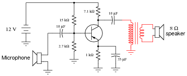
Question 41:
Each of the following faults will cause this audio amplifier circuit to stop working. Determine what diagnostic voltage measurement(s) would positively identify each one of the faults.

|
|
- �
- Microphone coil fails open:
- �
- Capacitor C1 fails shorted:
- �
- Resistor R1 fails open:
- �
- Resistor R2 fails open:
- �
- Capacitor C3 fails open:
- �
- Transformer T1 primary winding fails open:
- �
- Microphone coil fails open: No AC voltage at all across microphone terminals when sound is present.
- �
- Capacitor C1 fails shorted: DC voltage present across microphone terminals.
- �
- Resistor R1 fails open: Full DC supply voltage dropped across R1, no DC voltage dropped across R2 (could indicate a shorted R2 as well - no way to tell unless a resistance measurement is taken).
- �
- Resistor R2 fails open: Increased DC voltage drop across R2, decreased DC voltage drop across R1, reasonable transistor DC voltages (VE 0.7 volts less than VB, VC as expected based on value of VE and R3, R4 values) indicate that Q1 is probably not the source of the trouble.
- �
- Capacitor C3 fails open: Larger-than-normal AC voltage at collector terminal, with no AC voltage present across transformer primary winding.
- �
- Transformer T1 primary winding fails open: Larger-than-normal AC voltage across transformer primary winding, with no AC voltage across transformer secondary winding.
Notes:
The purpose of this question is to approach the domain of circuit troubleshooting from a perspective of knowing what the fault is, rather than only knowing what the symptoms are. Although this is not necessarily a realistic perspective, it helps students build the foundational knowledge necessary to diagnose a faulted circuit from empirical data. Questions such as this should be followed (eventually) by other questions asking students to identify likely faults based on measurements.
Question 42:
Suppose this microphone amplifier circuit used to function fine, but now has stopped outputting any sound at all:
|
|
Initial diagnostic measurements show all quiescent (DC) voltages to be normal. From this data, where would you suspect the problem is, and where would you suspect the problem is not?
Notes:
Ask your students why the normal DC voltage measurements indicate healthy resistors and transistor. How can we quickly eliminate those components as being faulty based on simple DC voltage measurements?
Question 43:
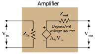
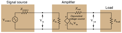
Sometimes you will see amplifier circuits expressed as collections of impedances and dependent sources:
|
|
With this model, the amplifier appears as a load (Zin) to whatever signal source its input is connected to, boosts that input voltage by the gain factor (AV), then outputs the boosted signal through a series output impedance (Zout) to whatever load is connected to the output terminals:
|
|
Explain why all these impedances (shown as resistors) are significant to us as we seek to apply amplifier circuits to practical applications. Which of these impedances do you suppose are typically easier for us to change, if they require changing at all?
Notes:
This question has multiple purposes: to introduce students to the modeling concept of a dependent source, to show how an amplifier circuit may be modeled using such a dependent source, and to probe into the importance of impedances in a complete amplification system: source, amplifier, and load. Many interesting things to discuss here!
Question 44:
Complete the table of output voltages, output currents, and input currents for several given values of input voltage in this common-collector amplifier circuit. Assume that the transistor is a standard silicon NPN unit, with a nominal base-emitter junction forward voltage of 0.7 volts:
|
|
-
Vin Vout Iin Iout
0.8 V
1.5 V
3.0 V
4.5 V
6.0 V
7.5 V
Calculate the amount of impedance ßeen" by the input voltage source Vin, given the following definition for impedance:
|
-
Vin Vout Iin Iout
0.8 V 0.1 V 2.80 mA 0.213 mA
1.5 V 0.8 V 22.4 mA 1.70 mA
3.0 V 2.3 V 64.4 mA 4.89 mA
4.5 V 3.8 V 106 mA 8.09 mA
6.0 V 5.3 V 148 mA 11.3 mA
7.5 V 6.8 V 190 mA 14.5 mA
|
Notes:
The purpose of this question, besides providing practice for common-collector circuit DC analysis, is to show the current-amplification properties of the common-collector amplifier. This is an important feature, as there is no voltage amplification in this type of amplifier circuit.
This approach to determining transistor amplifier circuit impedance is one that does not require prior knowledge of amplifier configurations. In order to obtain the necessary data to calculate voltage gain, all one needs to know are the "first principles" of Ohm's Law, Kirchhoff's Laws, and basic operating principles of a bipolar junction transistor. This question is really just a thought experiment: exploring an unknown form of circuit by applying known rules of circuit components. If students doubt the efficacy of "thought experiments," one need only to reflect on the success of Albert Einstein, whose thought experiments as a patent clerk (without the aid of experimental equipment) allowed him to formulate the basis of his Theories of Relativity.
Question 45:
Calculate the approximate input impedance (Zin) of this amplifier circuit:
|
|
Also, explain why input impedance is an important factor in amplifier circuits.
I won't directly tell you why input impedance is an important factor for amplifier circuits, but I'll give you a hint: Maximum Power Transfer Theorem.
Notes:
Ask you students to compare the input impedance of this amplifier with the load impedance. Does the transistor "match" impedances like a transformer does? Ask them to explain both the similarities and the differences between transformers and transistors as impedance-matching devices.
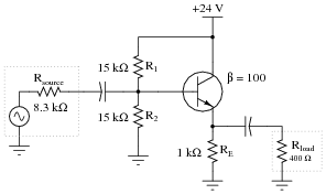
Question 46:
The voltage divider network employed to create a DC bias voltage for many transistor amplifier circuits has its own effect on amplifier input impedance. Without considering the presence of the transistor or the emitter resistance, calculate the impedance as ßeen" from the input terminal resulting from the two resistors R1 and R2 in the following common-collector amplifier circuit:
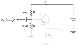
|
|
Remember, what you are doing here is actually determining the Thévenin/Norton equivalent resistance as seen from the input terminal by an AC signal. The input coupling capacitor reactance is generally small enough to be safely ignored.
Next, calculate the input impedance of the same circuit, this time considering the presence of the transistor and emitter resistor, assuming a current gain (b or hfe) of 60, and the following formula for impedance at the base resulting from b and RE:
|
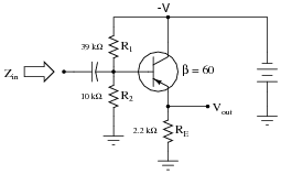
|
|
Develop an equation from the steps you take in calculating this impedance value.
Zin (complete circuit) � 7.514 kW
|
Notes:
This question is primarily an exercise in applying Thévenin's theorem to the amplifier circuit. The most confusing point of this for most students seems to be how to regard the DC power supply. A review of Thévenin equivalent circuit procedures and calculations might be in order here.
To be proper, the transistor's dynamic emitter resistance (r�e) could also be included in this calculation, but this just makes things more complex. For this question, I wanted to keep things as simple as possible by just having students concentrate on the issue of integrating the voltage divider impedance with the transistor's base impedance. With an emitter resistor value of 1500 ohms, the dynamic emitter resistance is negligibly small anyway.
Question 47:
The voltage divider network employed to create a DC bias voltage for many transistor amplifier circuits has its own effect on amplifier input impedance. Without considering the presence of the transistor or the emitter resistance, calculate the impedance as ßeen" from the input terminal resulting from the two resistors R1 and R2 in the following common-collector amplifier circuit:
|
|
Remember, what you are doing here is actually determining the Thévenin/Norton equivalent resistance as seen from the input terminal by an AC signal (consider the coupling capacitor reactance to be negligibly small).
Next, calculate the input impedance of the same circuit, this time considering the presence of the transistor and emitter resistor, assuming a current gain (b or hfe) of 42:
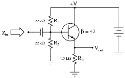
|
|
Develop an equation from the steps you take in calculating this impedance value.
Zin (complete circuit) � 9.4 kW
|
Notes:
This question is primarily an exercise in applying Thévenin's theorem to the amplifier circuit. The most confusing point of this for most students seems to be how to regard the DC power supply. A review of Thévenin equivalent circuit procedures and calculations might be in order here.
To be proper, the transistor's dynamic emitter resistance (r�e) could also be included in this calculation, but this just makes things more complex. For this question, I wanted to keep things as simple as possible by just having students concentrate on the issue of integrating the voltage divider impedance with the transistor's base impedance. With an emitter resistor value of 1500 ohms, the dynamic emitter resistance is negligibly small anyway.
Question 48:
Determining the output impedance of a common-emitter amplifier is impossible unless we know how to model the transistor in terms of components whose behavior is simple to express.
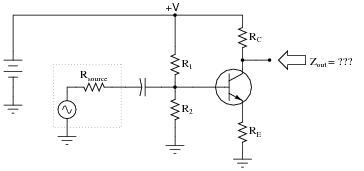
|
|
When in its active mode, a transistor operates like a current regulator. This is similar enough to the behavior of a current source that we may use a source to model the transistor's behavior for the sake of this impedance determination:
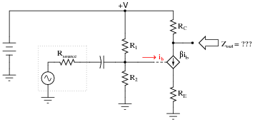
|
|
Now, apply the same steps you would use in determining the Thévenin or Norton equivalent impedance to the output of this amplifier circuit, and this will yield the amplifier's output impedance. Draw an equivalent circuit for the amplifier during this Thévenizing/Nortonizing process to show how the output impedance is determined.
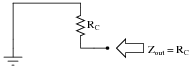
|
|
I'm leaving it up to you to explain why the amplifier circuit reduces to something as simple as this!
Follow-up question: what is the significance of showing the transistor as a current source using a diamond-shaped symbol rather than a circle? You should be familiar by now with circular current source symbols, but what does a diamond-shaped current source symbol specifically represent in a schematic diagram?
Notes:
The main problem students usually have when Thévenizing or Nortonizing this circuit is what to do with the current source. They may remember that voltage sources become shorted during the impedance-determination process, but usually make the mistake of doing the exact same thing with current sources. Remind your students if necessary that each source is to be replaced by its respective internal impedance. For voltage sources (with zero internal impedance, ideally) it means replacing them with short circuits. For current sources (with infinite internal impedance, ideally) it means replacing them with open circuits.
Question 49:
What is the ideal amount of load impedance for this amplifier circuit, so that maximum power will be delivered to it?
|
|
Suppose we wished to drive an 8 ohm audio speaker with this amplifier circuit. How could we better match the amplifier's impedance to the speaker's?
To match this amplifier to an 8 W speaker, we could use a matching transformer, or (better yet) a common-collector final transistor stage.
Notes:
Ask your students to explain whether they would connect a matching transformer as a step-up or a step-down to match source and load impedances in this example. How do we know which way we need to use the transformer?
Challenge your students by asking them how they might calculate the necessary transformer winding ratio for this impedance matching application. I wouldn't be surprised if many of your students do not remember the impedance ratio relationship to turns ratio back from their education in AC circuit theory. However, they should remember how turns ratio relates to voltage and current ratios, and from this they should be able to figure out the impedance transformation ratio of a transformer!
An important skill to have is the ability to reconstruct forgotten information by setting up "thought experiments" and deriving results from known (remembered) principles. I can't tell you how many times in my professional and academic life that this skill has been helpful to me.
Question 50:
Calculate the ideal amount of load impedance for this amplifier circuit, so that maximum power will be delivered to it:
|
|
Notes:
Ask your students to explain the mathematics behind this answer. What procedure gives them the quantity of 33 W from the given component values? Why is this answer only approximate? What factors might affect it?
Also, ask your students to explain why the common-collector transistor stage does not require a biasing network or coupling capacitor, as the common-emitter stage does.
Question 51:
Explain each of the mathematical approximations for this typical common-collector amplifier circuit:
|
|
|
|
|
What does each term in each expression represent, and why do they relate to one another as shown?
Notes:
The approximations for voltage gain, input impedance, and output impedance vary somewhat according to how precise the author(s) intended them to be. What you see here may be simpler or more complex than what you find in your textbook(s). The purpose of this question is to summarize gain and impedance calculations for this type of amplifier circuit, as well as to stimulate thought and discussion on the rationale for each. If students simply try to memorize these equations, they will forget them soon afterward. If they understand why each one is as it is from principles previously learned, both comprehension and retention will be much improved.
Question 52:
In a common-collector transistor amplifier circuit with voltage divider biasing, the input impedance (Zin) is a function of load impedance, emitter resistance (RE), and the two biasing resistances (R1 and R2). Often, the biasing resistances are of sufficiently low value to swamp the input impedance of the transistor, so that R1 and R2 constitute the heaviest load for any input signals driving the amplifier.
|
|
|
This is a shame, because the only practical purpose served by R1 and R2 is to provide a stable bias voltage so the transistor always functions in class A mode. In order to provide a stable bias, these resistors have to be relatively low in value compared to the impedance seen at the base of the transistor (resulting from the load). Otherwise, changes in dynamic emitter resistance (r�e) could result in significant bias shifts. So, the naturally high input impedance of the common-collector transistor configuration is spoiled by the necessary presence of R1 and R2.
A clever way to recover some of that naturally large input impedance is to add a bit of regenerative (positive) feedback to the circuit in the form of a capacitor and another resistor. This technique is given an equally clever name: bootstrapping.
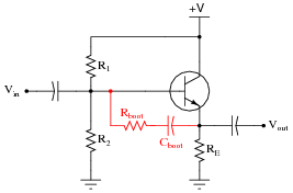
|
|
Explain how bootstrapping works, and why that particular name is given to the technique.
Notes:
Bootstrapping is an oft-used technique to boost amplifier input impedance, and it hints at the amazing potential of signal feedback in amplifier circuits. You might want to mention that bootstrapping is practical only if the feedback gain is slightly less than 1. If there is too much positive feedback, the amplifier will turn into an oscillator!
Question 53:
A common set of equations for calculating input and output impedances of common-collector amplifier circuits is as follows:
|
|
If precision is not required, we may greatly simplify these equations by assuming the transistor to be ideal; i.e. having an infinite current gain (b = �). Re-write these equations accordingly, and explain how you simplified each one.
|
|
Much simpler, don't you think?
Notes:
The purpose of this question is for students to see how (more) approximate predictions for circuits may be obtained through simplification. A good exercise is to calculate impedances for a given amplifier circuit using both the original and the simplified equations, to see just how äpproximate" the simplified answers are. Knowing how to eliminate complicated terms in equations (and what terms may be safely eliminated!) is key to estimating in the absence of a calculator.
Question 54:
Approximate the following values for this common-collector amplifier circuit, assuming the use of a silicon transistor:
|
|
- �
- AV (as a ratio) �
- �
- AV (in decibels) �
- �
- Zin �
- �
- Zout �
- �
- AV (as a ratio) � 1
- �
- AV (in decibels) � 0 dB
- �
- Zin � 5.962 kW
- �
- Zout � 39.6 W
Follow-up question: how would these figures change, if at all, supposing the transistor had an infinite current gain (b = �)?
Notes:
Nothing much to comment on here - just some practice on common-collector amplifier calculations. In calculating the dynamic emitter resistance, the following assumptions were taken:
- �
- r�e = 25 mV / IE
- �
- 0.7 volts drop (exactly) across base-emitter junction.
- �
- Negligible loading of bias voltage divider by the emitter resistance.
After calculating r�e, the following equations were used to approximate the impedances:
|
|
This question lends itself well to group discussions on component failure scenarios. After discussing how to calculate the requested values, you might want to ask students to consider how these values would change given some specific component failures (open resistors, primarily, since this is perhaps the most common way that a resistor could fail).
Question 55:
Explain each of the mathematical approximations for this typical common-emitter amplifier circuit (with a bypass capacitor):
|
|
|
|
|
What does each term in each expression represent, and why do they relate to one another as shown?
Notes:
The approximations for voltage gain, input impedance, and output impedance vary somewhat according to how precise the author(s) intended them to be. What you see here may be simpler or more complex than what you find in your textbook(s). The purpose of this question is to summarize gain and impedance calculations for this type of amplifier circuit, as well as to stimulate thought and discussion on the rationale for each. If students simply try to memorize these equations, they will forget them soon afterward. If they understand why each one is as it is from principles previously learned, both comprehension and retention will be much improved.
Question 56:
Explain each of the mathematical approximations for this typical common-emitter amplifier circuit (with the dynamic emitter resistance ßwamped" by RE):
|
|
|
|
|
What does each term in each expression represent, and why do they relate to one another as shown?
Notes:
The approximations for voltage gain, input impedance, and output impedance vary somewhat according to how precise the author(s) intended them to be. What you see here may be simpler or more complex than what you find in your textbook(s). The purpose of this question is to summarize gain and impedance calculations for this type of amplifier circuit, as well as to stimulate thought and discussion on the rationale for each. If students simply try to memorize these equations, they will forget them soon afterward. If they understand why each one is as it is from principles previously learned, both comprehension and retention will be much improved.
Question 57:
A common set of equations for calculating input and output impedances of bypassed common-emitter amplifier circuits is as follows:
|
|
If precision is not required, we may greatly simplify the first equation by assuming the transistor to be ideal; i.e. having an infinite current gain (b = �). Re-write the first equation accordingly, and explain how you simplified it.
|
Follow-up question: how does the similar simplification of the ßwamped" common-emitter amplifier's input impedance equation compare?
|
Notes:
The purpose of this question is for students to see how (more) approximate predictions for circuits may be obtained through simplification. A good exercise is to calculate impedances for a given amplifier circuit using both the original and the simplified equations, to see just how äpproximate" the simplified answers are. Knowing how to eliminate complicated terms in equations (and what terms may be safely eliminated!) is key to estimating in the absence of a calculator.
Question 58:
Approximate the following values for this common-emitter amplifier circuit, assuming the use of a silicon transistor:
|
|
- �
- AV (as a ratio) �
- �
- AV (in decibels) �
- �
- Zin �
- �
- Zout �
- �
- AV (as a ratio) � 112.5
- �
- AV (in decibels) � 41.02 dB
- �
- Zin � 2.175 kW
- �
- Zout � 9.1 kW
Follow-up question: how would these figures change, if at all, supposing the transistor had an infinite current gain (b = �)?
Notes:
Nothing much to comment on here - just some practice on common-emitter amplifier calculations. In calculating the dynamic emitter resistance, the following assumptions were taken:
- �
- r�e = 25 mV / IE
- �
- 0.7 volts drop (exactly) across base-emitter junction.
- �
- Negligible loading of bias voltage divider by the emitter resistance.
After calculating r�e, the following equations were used to approximate the impedances:
|
|
Voltage gain was approximated through the use of this equation:
|
This question lends itself well to group discussions on component failure scenarios. After discussing how to calculate the requested values, you might want to ask students to consider how these values would change given some specific component failures (open resistors, primarily, since this is perhaps the most common way that a resistor could fail).
Question 59:
A parasitic property of semiconductor PN junctions is capacitance across the depletion regions. This is often referred to as the Miller Effect. In transistor circuits, the Miller effect contributes to a decrease in voltage gain as signal frequency increases.
Explain why junction capacitances make the voltage gain of an amplifier decrease with increasing frequency.
Challenge question: is there any way you can think of to cancel out this negative feedback in an amplifier circuit?
Notes:
Ask your students to explain what a "negative feedback loop" is, and how exactly the base-collector junction capacitance forms one in a transistor circuit. Also, review the formula for capacitive reactance (XC), and ask your students to relate this frequency dependence to the degree of negative feedback established in an amplifier circuit.
The challenge question may be answered with a little research into the Miller-effect. There is a method for cancellation of this unwanted negative feedback loop, but it may not be possible to implement in all amplifier circuit topologies.
Question 60:
The BJT amplifier configuration most affected by the Miller effect at high frequencies is the common-emitter. Common-collector and common-base amplifier configurations do not suffer the same great losses of voltage gain at high frequency as the common-emitter circuit does. After examining the following amplifier circuits (with the Miller effect capacitance shown external to the transistors), explain why:
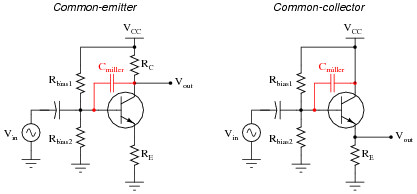
|
|
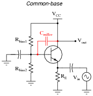
|
|
The common-base circuit is interesting: it would seem there is a possibility for negative feedback through the Miller capacitance here, from the collector to the base. However, since the base terminal is effectively grounded (as far as AC signals are concerned) by the bypass capacitor, any feedback through the Miller capacitance becomes shunted straight to ground where is has no effect on the amplifier's operation.
Notes:
Here I give more explanation than is usual for me, because the concept is not easy to understand, and is often presented in a muddled fashion by textbooks.
Question 61:
The "Miller capacitance" of a transistor in a common-emitter configuration is often expressed as the product of the transistor's base-to-collector junction capacitance (CBC) and b+1:
|
Why is this? What purpose does it serve to include the transistor's gain into the calculation, rather than just expressing the junction capacitance as it is?
|
Notes:
This effect of base-collector capacitance "multiplication," while being a nuisance in typical amplifier applications, may be exploited for positive benefit in other circuits. Many an op-amp circuit has been built specifically to "multiply" the value of a passive component, when some exceptionally large value is needed that will not fit on a circuit board. This technique has its limits, of course, but is good to keep in mind.
Some students may not be familiar with the double-chevron notation ( >> or << ). It means much greater than, and much less than, respectively.
Question 62:
An important performance parameter for amplifier circuits is bandwidth. Explain what "bandwidth" means, and what factor(s) limit the bandwidth for electronic amplifiers.
|
|
Rolloff at the high-frequency end is largely due to the Miller effect, while rolloff at the low-frequency end is usually due to coupling capacitors in the circuit.
Notes:
If the graph given in the answer reminds students of a band-pass filter, then they have been paying attention!