Bipolar transistor biasing circuits
Question 1:
| Don't just sit there! Build something!! |
Learning to mathematically analyze circuits requires much study and practice. Typically, students practice by working through lots of sample problems and checking their answers against those provided by the textbook or the instructor. While this is good, there is a much better way.
You will learn much more by actually building and analyzing real circuits, letting your test equipment provide the änswers" instead of a book or another person. For successful circuit-building exercises, follow these steps:
- 1.
- Carefully measure and record all component values prior to circuit construction, choosing resistor values high enough to make damage to any active components unlikely.
- 2.
- Draw the schematic diagram for the circuit to be analyzed.
- 3.
- Carefully build this circuit on a breadboard or other convenient medium.
- 4.
- Check the accuracy of the circuit's construction, following each wire to each connection point, and verifying these elements one-by-one on the diagram.
- 5.
- Mathematically analyze the circuit, solving for all voltage and current values.
- 6.
- Carefully measure all voltages and currents, to verify the accuracy of your analysis.
- 7.
- If there are any substantial errors (greater than a few percent), carefully check your circuit's construction against the diagram, then carefully re-calculate the values and re-measure.
When students are first learning about semiconductor devices, and are most likely to damage them by making improper connections in their circuits, I recommend they experiment with large, high-wattage components (1N4001 rectifying diodes, TO-220 or TO-3 case power transistors, etc.), and using dry-cell battery power sources rather than a benchtop power supply. This decreases the likelihood of component damage.
As usual, avoid very high and very low resistor values, to avoid measurement errors caused by meter "loading" (on the high end) and to avoid transistor burnout (on the low end). I recommend resistors between 1 kW and 100 kW.
One way you can save time and reduce the possibility of error is to begin with a very simple circuit and incrementally add components to increase its complexity after each analysis, rather than building a whole new circuit for each practice problem. Another time-saving technique is to re-use the same components in a variety of different circuit configurations. This way, you won't have to measure any component's value more than once.
Notes:
It has been my experience that students require much practice with circuit analysis to become proficient. To this end, instructors usually provide their students with lots of practice problems to work through, and provide answers for students to check their work against. While this approach makes students proficient in circuit theory, it fails to fully educate them.
Students don't just need mathematical practice. They also need real, hands-on practice building circuits and using test equipment. So, I suggest the following alternative approach: students should build their own "practice problems" with real components, and try to mathematically predict the various voltage and current values. This way, the mathematical theory "comes alive," and students gain practical proficiency they wouldn't gain merely by solving equations.
Another reason for following this method of practice is to teach students scientific method: the process of testing a hypothesis (in this case, mathematical predictions) by performing a real experiment. Students will also develop real troubleshooting skills as they occasionally make circuit construction errors.
Spend a few moments of time with your class to review some of the "rules" for building circuits before they begin. Discuss these issues with your students in the same Socratic manner you would normally discuss the worksheet questions, rather than simply telling them what they should and should not do. I never cease to be amazed at how poorly students grasp instructions when presented in a typical lecture (instructor monologue) format!
A note to those instructors who may complain about the "wasted" time required to have students build real circuits instead of just mathematically analyzing theoretical circuits:
What is the purpose of students taking your course?
If your students will be working with real circuits, then they should learn on real circuits whenever possible. If your goal is to educate theoretical physicists, then stick with abstract analysis, by all means! But most of us plan for our students to do something in the real world with the education we give them. The "wasted" time spent building real circuits will pay huge dividends when it comes time for them to apply their knowledge to practical problems.
Furthermore, having students build their own practice problems teaches them how to perform primary research, thus empowering them to continue their electrical/electronics education autonomously.
In most sciences, realistic experiments are much more difficult and expensive to set up than electrical circuits. Nuclear physics, biology, geology, and chemistry professors would just love to be able to have their students apply advanced mathematics to real experiments posing no safety hazard and costing less than a textbook. They can't, but you can. Exploit the convenience inherent to your science, and get those students of yours practicing their math on lots of real circuits!
Question 2:
Complete the table of output voltages for several given values of input voltage in this common-collector amplifier circuit. Assume that the transistor is a standard silicon NPN unit, with a nominal base-emitter junction forward voltage of 0.7 volts:
|
|
-
Vin Vout
0.0 V
0.5 V
1.0 V
1.5 V
5.0 V
7.8 V
Based on the values you calculate, explain why the common-collector circuit configuration is often referred to as an emitter follower.
-
Vin Vout
0.0 V 0.0 V
0.5 V 0.0 V
1.0 V 0.3 V
1.5 V 0.8 V
5.0 V 4.3 V
7.8 V 7.1 V
The voltage at the transistor's emitter terminal approximately "follows" the voltage applied to the base terminal, hence the name.
Notes:
At first, the ëmitter follower" transistor circuit may seem pointless, since the output voltage practically equals the input voltage (especially for input voltages greatly exceeding 0.7 volts DC). "What possible good is a circuit like this?" some of your students may ask. The answer to this question, of course, has to do with currents in the circuit, and not necessarily voltages.
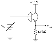
Question 3:
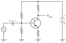
Describe what the output voltage of this transistor circuit will do (measured with reference to ground), if the potentiometer wiper begins at the full-down position (common with ground), and is slowly moved in the upward direction (closer to +V):
|
|
Follow-up question: based on this result, would you be inclined to call this amplifier an inverting or a noninverting circuit?
Notes:
Although this circuit is very simple, it is also very important to master. Be sure to discuss its operation thoroughly with your students, so they understand.
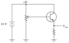
Question 4:
Describe what the output voltage of this transistor circuit will do (measured with reference to ground), if the input voltage ramps from 0 volts to -10 volts (measured with respect to ground):
|
|
Notes:
This might not be the result many students expect! It is important, though, for them to understand the importance of polarity in transistor circuits. This example should make that abundantly clear.
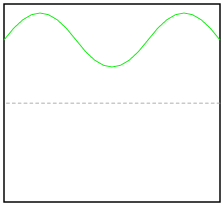
Question 5:
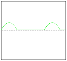
If we were to apply a sinusoidal AC signal to the input of this transistor amplifier circuit, the output would definitely not be sinusoidal:
|
|
It should be apparent that only portions of the input are being reproduced at the output of this circuit. The rest of the waveform seems to be "missing," being replaced by a flat line. Explain why this transistor circuit is not able to amplify the entire waveform.
Notes:
Sometimes it is helpful for students to re-draw the circuit using a transistor model showing the base-emitter junction as a diode. If you think this model would help some of your students understand the concept here, have another student draw the transistor model on the whiteboard, and use that drawing as a discussion aid. Like any PN junction, the base-emitter junction of a BJT only "wants" to conduct current in one direction.
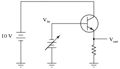
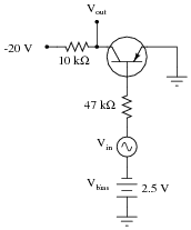
Question 6:
Class-A operation may be obtained from this simple transistor circuit if the input voltage (Vin) is "biased" with a series-connected DC voltage source:
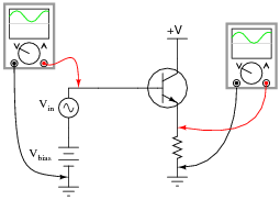
|
|
First, define what "Class A" amplifier operation is. Then, explain why biasing is required for this transistor to achieve it.
Notes:
A "trick" it may be, but a very useful and very common "trick" it is! Discuss this concept with your students at length, being sure they have ample time and opportunity to ask questions of their own.
One question that may arise is, "how much DC bias voltage is necessary?" If no one asks this question, ask it yourself! Discuss with your students what would constitute the minimum amount of bias voltage necessary to ensure the transistor never goes into "cutoff" anywhere in the waveform's cycle, and also the maximum bias voltage to prevent the transistor from ßaturating".
Question 7:
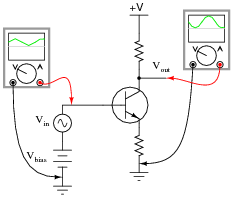
Explain how the following bias networks function:
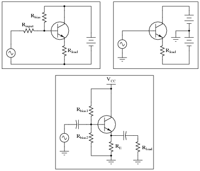
|
|
Each one has the same basic purpose, but works in a different way to accomplish it. Describe the purpose of any biasing network in an AC signal amplifier, and comment on the different means of accomplishing this purpose employed by each of the three circuits.
Hint: imagine if the AC signal source in each circuit were turned off (replaced with a short). Explain how each biasing network maintains the transistor in a partially ön" state at all times even with no AC signal input.
Notes:
All three biasing techniques are commonly used in transistor amplifier circuitry, so it behooves each student to understand them well. In each case, resistors provide a "trickle" of current through the base of the transistor to keep it turned partially ön" at all times.
One exercise you might have your students do is come up to the board in front of the room and draw an example of this circuit, then everyone may refer to the drawn image when discussing the circuit's characteristics.
Question 8:
Describe what the output voltage of this transistor circuit will do (measured with reference to ground), if the potentiometer wiper begins at the full-down position (common with ground), and is slowly moved in the upward direction (closer to +V):
|
|
Follow-up question: based on this result, would you be inclined to call this amplifier an inverting or a noninverting circuit?
Notes:
Although this circuit is very simple, it is also very important to master. Be sure to discuss its operation thoroughly with your students, so they understand.
Question 9:
If we were to apply a sinusoidal AC signal to the input of this transistor amplifier circuit, the output would definitely not be sinusoidal:
|
|
It should be apparent that only portions of the input are being amplified in this circuit. The rest of the waveform seems to be "missing" in the output, being replaced by a flat line. Explain why this transistor circuit is not able to amplify the entire waveform.
Notes:
Sometimes it is helpful for students to re-draw the circuit using a transistor model showing the base-emitter junction as a diode. If you think this model would help some of your students understand the concept here, have another student draw the transistor model on the whiteboard, and use that drawing as a discussion aid. Like any PN junction, the base-emitter junction of a BJT only "wants" to conduct current in one direction.
Question 10:
Class-A operation may be obtained from this simple transistor circuit if the input voltage (Vin) is "biased" with a series-connected DC voltage source:
|
|
First, define what "Class A" amplifier operation is. Then, explain why biasing is required for this transistor to achieve it.
Notes:
A "trick" it may be, but a very useful and very common "trick" it is! Discuss this concept with your students at length, being sure they have ample time and opportunity to ask questions of their own.
One question that may arise is, "how much DC bias voltage is necessary?" If no one asks this question, ask it yourself! Discuss with your students what would constitute the minimum amount of bias voltage necessary to ensure the transistor never goes into "cutoff" anywhere in the waveform's cycle, and also the maximum bias voltage to prevent the transistor from ßaturating".
Question 11:
Explain how the following bias networks function:
|
|
Each one has the same basic purpose, but works in a different way to accomplish it. Describe the purpose of any biasing network in an AC signal amplifier, and comment on the different means of accomplishing this purpose employed by each of the three circuits.
Notes:
All three biasing techniques are commonly used in transistor amplifier circuitry, so it behooves each student to understand them well. In each case, resistors provide a "trickle" of current through the base of the transistor to keep it turned partially ön" at all times.
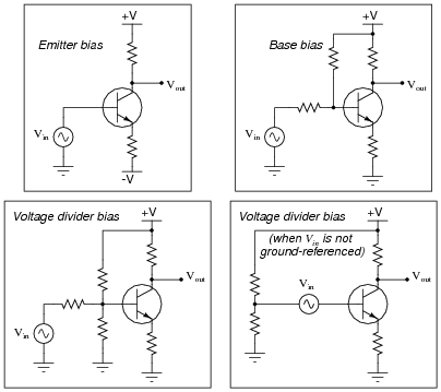
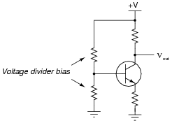
Question 12:
A very common method of providing bias voltage for transistor amplifier circuits is with a voltage divider:
|
|
However, if we were to directly connect a source of AC signal voltage to the junction between the two voltage divider resistors, the circuit would most likely function as if there were no voltage divider network in place at all:
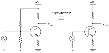
|
|
Instead, circuit designers usually place a coupling capacitor between the signal source and the voltage divider junction, like this:
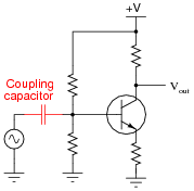
|
|
Explain why a coupling capacitor is necessary to allow the voltage divider to work in harmony with the AC signal source. Also, identify what factors would be relevant in deciding the size of this coupling capacitor.
If this concept is still not clear, consider this circuit:
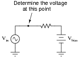
|
|
As far as capacitor size is concerned, it should be large enough that its reactance is negligible. I'll let you determine what factors define negligibility in this context!
Follow-up question: which voltage source (AC or DC?) "wins" at the point specified in the above circuit? Explain why this is so, and then show how a suitably located capacitor would allow both voltage signals to co-exist at that point.
Notes:
Many beginning students experience difficulty understanding the purpose of the coupling capacitor, and transistor amplifier biasing in general. Be sure to spend plenty of time discussing the principle of this circuit, because it is very commonplace in transistor circuitry.
Question 13:
Explain how it is possible for a fault in the biasing circuitry of a transistor amplifier to completely kill the (AC) output of that amplifier. How and why can a shift in DC bias voltage have an effect on the AC signal being amplified?
Notes:
This question asks students to explore the possibility of complete AC signal failure due to a simple shift in DC bias, based on their understanding of how transistor amplifiers function. It may seem paradoxical that such a ßmall" fault could have such a large effect on an amplifier circuit, but it should make sense once students grasp how important bias is to class-A amplifier operation.
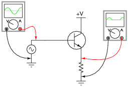
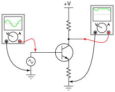
Question 14:
A student builds the following circuit and connects an oscilloscope to its output:
|
|
The waveform shown on the oscilloscope display looks like this:
|
|
Definitely not Class-A operation! Suspecting a problem with the input waveform, the student disconnects the oscilloscope probe from the amplifier output and moves it over to the amplifier input terminal. There, the following waveform is seen:
|
|
How can this amplifier circuit be producing such a distorted output waveform with such a clean input waveform? Explain your answer.
Notes:
Ask your students how they can tell the difference between excessive biasing and insufficient biasing, by inspection of the output waveform. There is a difference to be seen, but it requires a good understanding of how the circuit works! Students may be tempted to simply memorize waveforms ("when I see this kind of waveform, I know the problem is excessive biasing . . ."), so prepare to challenge their understanding with questions such as:
- �
- What polarity of input signal drives the transistor toward cutoff?
- �
- What polarity of input signal drives the transistor toward saturation?
- �
- Where on the output waveform is the transistor in cutoff (if at all)?
- �
- Where on the output waveform is the transistor in saturation (if at all)?
- �
- Where on the output waveform is the transistor in its active mode?
Another point worth mentioning: some students may be confused by the phasing of the input and output waveforms, comparing the two different oscilloscope displays. For a common-emitter (inverting) amplifier such as this, they expect to see the output voltage peak positive whenever the input voltage peaks negative, and visa-versa, but here the two oscilloscope displays show positive peaks occurring right next to the left-hand side of the screen. Why is this? Because the oscilloscope does not represent phase unless it is in dual-trace mode! When you disconnect the input probe and move it to another point in the circuit, any time reference is lost, the oscilloscope's triggering function placing the first waveform peak right where you tell it to, usually near the left-hand side of the display.
Question 15:
Suppose you were building a Class-A transistor amplifier for audio frequency use, but did not have an oscilloscope available to check the output waveform for the presence of "clipping" caused by improper biasing. You do, however, have a pair of audio headphones you may use to listen to the signals.
Explain how you would use a pair of headphones to check for the presence of severe distortion in a waveform.
Notes:
The answer I want for this question is not just a parroting of the answer I've given. Anyone can say ä distorted wave will sound different." I want to know how it sounds different, and this answer can only come by direct experimentation!
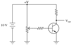
Question 16:
Calculate the approximate quiescent (DC) base current for this transistor circuit, assuming an AC input voltage of 0 volts, and a silicon transistor:
|
|
Notes:
This circuit was purposely drawn in a convoluted fashion to force students to identify its configuration apart from the standard layout. Many people lack the spatial reasoning skills to do this easily, and require a lot of practice before they become proficient. Ask your more proficient students if they have any "tips" for helping those who struggle with problems like these. Are there any simple methods which we may use to re-draw this circuit in an easier-to-understand form?
Question 17:
Calculate the potentiometer wiper voltage (Vbias) required to maintain the transistor right at the threshold between cutoff and active mode. Then, calculate the input voltage required to drive the transistor right to the threshold between active mode and saturation. Assume ideal silicon transistor behavior, with a constant b of 100:
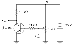
|
|
At the threshold between active mode and saturation, Vbias = -1.72 volts (assuming 0 volts VCE at saturation)
Follow-up question: if we were using the potentiometer to establish a bias voltage for an AC signal, what amount of DC bias voltage would place the transistor directly between these two extremes of operation (cutoff versus saturation), so as to allow the AC input signal to ßwing" equal amounts positive and negative at the distortion limit? In other words, what voltage setting is exactly between -0.7 volts and -1.72 volts?
Notes:
If your students are experiencing difficulty analyzing this circuit, ask them to begin by calculating the transistor currents at the thresholds of cutoff and saturation.
A mathematical trick I've found helpful through the years for finding the midpoint between two values is to add the two values together and then divide by two. Challenge your students to use other means of calculating this midpoint value, though.
Question 18:
When inserting a signal coupling capacitor into the bias network for this transistor amplifier, which way should the (polarized) capacitor go? (Hint: the AC signal source outputs pure AC, with a time-averaged DC value of 0 volts).
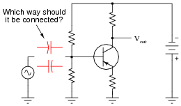
|
|
Explain why the orientation of this capacitor matters, and what might happen if it is connected the wrong way.
|
|
Notes:
It is easy to miss the detail of the power supply's polarity being "backward" from what is typically seen (negative instead of positive). Actually, I am surprised to see how many introductory textbooks have the coupling capacitor drawn the wrong way, so expect that some students may become confused by researching their texts for the answer!
Question 19:
Describe how proper biasing is accomplished in this headphone amplifier circuit (suitable for amplifying the audio output of a small radio):
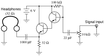
|
|
Also, describe the functions of the 10 kW potentiometer and the 22 mF capacitor.
Challenge question: there is a name used to describe the dual-transistor configuration used in this circuit, where a pair of PNP or NPN transistors is cascaded, with the emitter of one going to the base of the other. What is this name, and what advantage does this configuration provide over a single transistor?
Notes:
This circuit is simple enough to assemble and test in an hour or two, on a solderless breadboard. It would make a great lab experiment, and can be used by the students outside of class!
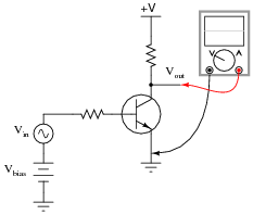
Question 20:
The following circuit is a three-channel audio mixer circuit, used to blend and amplify three different audio signals (coming from microphones or other signal sources):
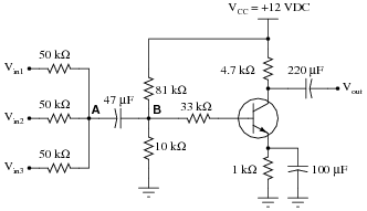
|
|
Suppose we measured a 9 kHz sinusoidal voltage of 0.5 volts (peak) at point Ä" in the diagram, using an oscilloscope. Determine the voltage at point "B" in the circuit, after this AC signal voltage "passes through" the voltage divider biasing network.
The voltage at point "B" will be a mix of AC and DC, so be sure to express both quantities! Ignore any "loading" effects of the transistor's base current on the voltage divider.
Notes:
Ask your students what purpose the 47 mF capacitor serves. Since its presence does not noticeably attenuate the AC signal at point Ä" (the whole 0.5 volts AC getting to point B), why not just replace it with a straight piece of wire?
Question 21:
Explain what is meant by the phrase, "Class-A amplifier operation." What does it mean for a particular amplifier circuit to operate in "Class-A" mode?
Notes:
Of course, the natural question following this one is, "What other classes of operation are there?" This would be an excellent time to preview Class-B (push-pull) and Class-C operations if time permits.