CMOS logic gates
Question 1:
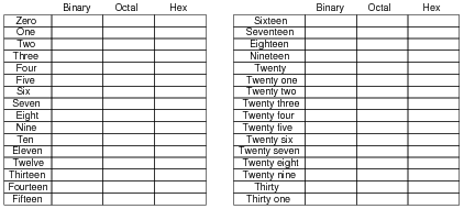
Counting practice: count from zero to thirty-one in binary, octal, and hexadecimal:
|
|
Notes:
In order to familiarize students with these ßtrange" numeration systems, I like to begin each day of digital circuit instruction with counting practice. Students need to be fluent in these numeration systems by the time they are finished studying digital circuits!
One suggestion I give to students to help them see patterns in the count sequences is "pad" the numbers with leading zeroes so that all numbers have the same number of characters. For example, instead of writing "10" for the binary number two, write "00010". This way, the patterns of character cycling (especially binary, where each successively higher-valued bit has half the frequency of the one before it) become more evident to see.
Question 2:
| Don't just sit there! Build something!! |
Learning to analyze digital circuits requires much study and practice. Typically, students practice by working through lots of sample problems and checking their answers against those provided by the textbook or the instructor. While this is good, there is a much better way.
You will learn much more by actually building and analyzing real circuits, letting your test equipment provide the änswers" instead of a book or another person. For successful circuit-building exercises, follow these steps:
- 1.
- Draw the schematic diagram for the digital circuit to be analyzed.
- 2.
- Carefully build this circuit on a breadboard or other convenient medium.
- 3.
- Check the accuracy of the circuit's construction, following each wire to each connection point, and verifying these elements one-by-one on the diagram.
- 4.
- Analyze the circuit, determining all output logic states for given input conditions.
- 5.
- Carefully measure those logic states, to verify the accuracy of your analysis.
- 6.
- If there are any errors, carefully check your circuit's construction against the diagram, then carefully re-analyze the circuit and re-measure.
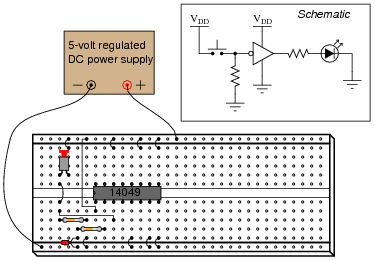
Always be sure that the power supply voltage levels are within specification for the logic circuits you plan to use. If TTL, the power supply must be a 5-volt regulated supply, adjusted to a value as close to 5.0 volts DC as possible.
One way you can save time and reduce the possibility of error is to begin with a very simple circuit and incrementally add components to increase its complexity after each analysis, rather than building a whole new circuit for each practice problem. Another time-saving technique is to re-use the same components in a variety of different circuit configurations. This way, you won't have to measure any component's value more than once.
Notes:
It has been my experience that students require much practice with circuit analysis to become proficient. To this end, instructors usually provide their students with lots of practice problems to work through, and provide answers for students to check their work against. While this approach makes students proficient in circuit theory, it fails to fully educate them.
Students don't just need mathematical practice. They also need real, hands-on practice building circuits and using test equipment. So, I suggest the following alternative approach: students should build their own "practice problems" with real components, and try to predict the various logic states. This way, the digital theory "comes alive," and students gain practical proficiency they wouldn't gain merely by solving Boolean equations or simplifying Karnaugh maps.
Another reason for following this method of practice is to teach students scientific method: the process of testing a hypothesis (in this case, logic state predictions) by performing a real experiment. Students will also develop real troubleshooting skills as they occasionally make circuit construction errors.
Spend a few moments of time with your class to review some of the "rules" for building circuits before they begin. Discuss these issues with your students in the same Socratic manner you would normally discuss the worksheet questions, rather than simply telling them what they should and should not do. I never cease to be amazed at how poorly students grasp instructions when presented in a typical lecture (instructor monologue) format!
I highly recommend CMOS logic circuitry for at-home experiments, where students may not have access to a 5-volt regulated power supply. Modern CMOS circuitry is far more rugged with regard to static discharge than the first CMOS circuits, so fears of students harming these devices by not having a "proper" laboratory set up at home are largely unfounded.
A note to those instructors who may complain about the "wasted" time required to have students build real circuits instead of just mathematically analyzing theoretical circuits:
What is the purpose of students taking your course?
If your students will be working with real circuits, then they should learn on real circuits whenever possible. If your goal is to educate theoretical physicists, then stick with abstract analysis, by all means! But most of us plan for our students to do something in the real world with the education we give them. The "wasted" time spent building real circuits will pay huge dividends when it comes time for them to apply their knowledge to practical problems.
Furthermore, having students build their own practice problems teaches them how to perform primary research, thus empowering them to continue their electrical/electronics education autonomously.
In most sciences, realistic experiments are much more difficult and expensive to set up than electrical circuits. Nuclear physics, biology, geology, and chemistry professors would just love to be able to have their students apply advanced mathematics to real experiments posing no safety hazard and costing less than a textbook. They can't, but you can. Exploit the convenience inherent to your science, and get those students of yours practicing their math on lots of real circuits!
Question 3:
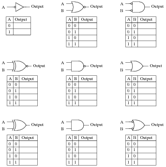
Identify each of these logic gates by name, and complete their respective truth tables:
|
|
|
|
Notes:
In order to familiarize students with the standard logic gate types, I like to given them practice with identification and truth tables each day. Students need to be able to recognize these logic gate types at a glance, or else they will have difficulty analyzing circuits that use them.
Question 4:
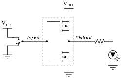
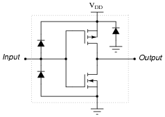
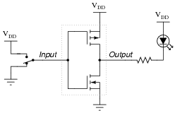
The simplest type of digital logic circuit is an inverter, also called an inverting buffer, or NOT gate. Here is a schematic diagram for an inverter gate constructed from complementary MOSFETs (CMOS), shown connected to a SPDT switch and an LED:
|
|
Determine the status of the LED in each of the input switch's two positions. Denote the logic level of switch and LED in the form of a truth table:

|
|

|
|
Notes:
Have your students explain the operation of this very simple MOSFET circuit, describing how the inverse logic state is generated at the output terminal, from a given input state. Discuss with your students the simplicity of the CMOS inverter, especially contrasted against a TTL inverter circuit.
Question 5:
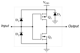
Practical CMOS logic gates contain more than just MOSFETs. Here is a schematic diagram for a typical inverter gate circuit, with protection diodes:
|
|
Explain what specific conditions each protection diode protects against.
Notes:
It is important that students realize these "protection" diodes do not allow circuit designers and builders to disregard good design practices with impunity. Ask your students, in each case, how each protection diode accomplishes its task of protecting the MOSFETs from damage. Does this mean the gate circuit will be able to withstand abnormal conditions indefinitely? Why or why not?
Question 6:
A student builds the following digital circuit on a solderless breadboard (a "proto-board"):
|
|
The DIP circuit is a hex inverter (it contains six ïnverter" or "NOT" logic gates), but only one of these gates is being used in this circuit. The student's intent was to build a logic circuit that energized the LED when the pushbutton switch was unactuated, and de-energized the LED when the switch was pressed: so that the LED indicates the reverse state of the switch itself. The student builds this circuit, and it is found to function perfectly well.
Explain the purpose of the resistor on the input of the inverter. What is it there for? What might happen if it were to be removed from the circuit?
Also, explain why the inputs of all the unused inverter gates in this IC have been either connected to ground or to VDD. Is this necessary for the circuit to work properly, or is it just a precautionary measure?
Shorting all unused gate inputs to either ground or VDD is merely a precautionary measure. It prevents unnecessary power draw from the supply, and possible IC overheating.
Notes:
Discuss the problem of "floating" or "high-Z" states with your students, especially in the context of CMOS. What is it about the nature of a CMOS circuit that makes floating inputs especially troublesome? Ask your students to contrast this against floating TTL inputs.
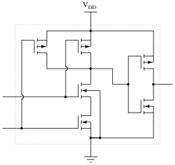
Question 7:
The following is an internal schematic of a CMOS logic gate. Based on your analysis of the transistor circuit, determine what type of gate (AND, OR, NAND, NOR, XOR, etc.) it is:
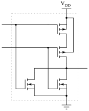
|
|
Follow-up question: identify a series of "thought experiments" you could perform on this circuit schematic to determine the identity of the gate. In other words, document what imagined conditions you would subject this gate to, and what the resulting output states would signify, in answering the question of what type of gate this is.
Notes:
CMOS logic gate circuits are the easiest of all the gates to analyze internally! Discuss with your students why the second-from-the-top MOSFET uses an independent substrate connection (as opposed to making it common with the source, as usual).
Question 8:
What is the typical power supply voltage range for a CD4xxx series (or MC4xxx series) CMOS logic gate? How does this compare with the allowable power supply voltage range for a standard (5 volt) TTL logic gate? Consult a datasheet for your answer.
Notes:
This question gets students in the habit of consulting datasheets to obtain information on logic gate circuits. Datasheets are a wealth of technical information, and students absolutely have to become adept at referencing them to obtain the information they need to build and troubleshoot logic circuits.
Question 9:
A logic probe is a very useful tool for working with digital logic circuits. It indicates "high" and "low" logic states by means of LED's, giving visual indication only if the voltage levels are appropriate for each state.
Here is a schematic diagram for a logic probe built using comparators. Each comparator has a threshold adjustment potentiometer, so that it may be set to indicate its respective logic state only if the signal voltage is well within the range stated by the logic manufacturer:
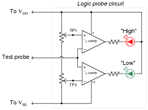
|
|
When this logic probe circuit is connected to the VDD and VSS power supply terminals of a powered CMOS circuit, what voltage levels should test points TP1 and TP2 be adjusted to, in order for the probe to properly indicate "high" and "low" CMOS logic states? Consult a datasheet for the quad NAND gate numbered 4011. This is a legacy CMOS integrated circuit.
Follow-up question: write a formula for calculating appropriate current-limiting resistor sizes for the two LEDs in this circuit, given the value of +V and the LED forward voltage and current values.
Challenge question: the logic probe circuit shown is minimal in component count. To make a more practical and reliable probe, one would probably want to have reverse-polarity protection (in case someone were to accidently connect the probe backward across the power supply) as well as decoupling for immunity against electrical noise. Add whatever necessary components you think there should be in this circuit to provide these features.
Notes:
The most obvious lesson of this question is to introduce (or review as the case may be) the purpose and operation of a logic probe. However, this question is also a veiled introduction (or review) of CMOS logic levels.
Question 10:
Here is a schematic diagram for a simple electronic combination lock, controlling power to a door lock solenoid:
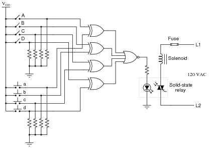
|
|
The four pushbutton switches (a, b, c, and d) are accessible to the person wishing to enter the door. The four toggle switches (A, B, C, and D) are located behind the door, and are used to set the code necessary for entering.
Explain how this system is supposed to work. What are the logic states of the respective gate outputs when a matching code is entered through the pushbutton switches? How about when a non-matching code is entered?
Do you see any security problems with this door lock circuit? How easy would it be for someone to enter, who does not know the four-bit code? Do you have any suggestions for improving this lock design?
Here is what I recommend as a strategy for improving the level of security offered by this system: install a fifth pushbutton switch as an Ënter" key. If someone enters the correct four-bit code and then pushes the Ënter" button, the door will open. However, if someone enters the wrong four-bit code and pushes the Ënter" button, the door will not open and a loud alarm will sound! This makes it "risky" to enter a wrong code, thus improving the security of the system.
Follow-up question: modify the circuit shown to implement an improved measure of security - either the strategy suggested or one of your own design.
Notes:
I strongly suggest you take the time to implement an improved-security design with your students. A practical project such as this sparks a lot of interest, and thus provides an excellent learning opportunity.
Not only does this question afford the opportunity to analyze logic gates, but it also provides a context in which to review optocouplers and TRIACs. Ask your students what the labels "L1" and "L2" mean, with reference to AC power circuitry, as well.
Question 11:
Many modern CMOS gate circuits are buffered with additional transistor stages on their outputs. For example, an unbuffered AND gate is shown here, with no more transistors than is necessary to fulfill the ÄND" logic function:
|
|
One type of "buffered" CMOS AND gate looks like this:
|
|
As far as the basic logic function is concerned, the additional transistors are unnecessary. However, the "buffering" they provide does serve a useful function. What is that function? Are there any disadvantages to buffered logic gates, versus unbuffered?
Follow-up question: identify the on/off states of all transistors in the buffered circuit for both (high and low) input conditions.
Notes:
Texas Instruments publishes an excellent application report (SCHA004 - October 2002) comparing buffered versus unbuffered CMOS logic gates. I highly recommend it for your reference.
Question 12:
In the early days of solid-state logic gate circuit technology, there was a very clear distinction between TTL and CMOS. TTL gates were capable of switching on and off very fast, required a tightly regulated power supply voltage, and used a lot of power. CMOS gates were not quite as fast as TTL, but could tolerate a much wider range of power supply voltages and were far less wasteful on power.
Then, during the 1980's a new technology known as high-speed CMOS, or HCMOS, entered the scene. Explain what HCMOS is, how it compares to the older TTL and CMOS families (54/74xx and 4xxx number series, respectively), and where it is often used. Hint: high-speed CMOS bears the same numerical codes as the old TTL 54xx and 74xx series ICs (e.g. 74HC00 instead of 7400).
Notes:
High-speed CMOS was a very important developmental milestone in digital logic gate technology, and it is essential for modern (2005) students of electronics to be aware of since it is so widely used. In many ways it blends the best of the old TTL and CMOS worlds, with few disadvantages.
Question 13:
In high-speed digital circuits, a very important logic gate parameter is propagation delay: the delay time between a change-of-state on a gate's input and the corresponding change-of-state on that gate's output. Consult a manufacturer's datasheet for any CMOS logic gate and report the typical propagation delay times published there.
Also, explain what causes propagation delay in logic gates. Why isn't the change in output state instantaneous when an input changes states?
Follow-up questions: What difference is there between high-to-low output transitions versus low-to-high output transitions for the gate you researched? Which transition is faster?
Notes:
I purposely omitted answers for this question, not only because I want students to do the research on their own, but also because it makes it more interesting when students consult different datasheets and derive different answers (for different logic "families")!
Question 14:
Logic gates are limited in the number of gate inputs which one output can reliably drive. This limit is referred to as fan-out:
|
|
Explain why this limit exists. What is it about the construction of CMOS logic gates that inherently limits the number of CMOS inputs that any one CMOS output can drive? What might happen if this limit is exceeded?
Fan-out for CMOS is a quite different than fan-out for TTL. Most importantly is that CMOS fan-out is inversely proportional to operating frequency. Explain why.
Notes:
For the relatively simple digital circuits that beginning students build, fan-out is rarely a problem. More likely is that students will try to drive a load that is too "heavy," causing the same voltage level problem.
Question 15:
An important parameter of logic gate circuitry is noise margin. What exactly is "noise margin," and how is it defined for logic gates?
Specifically, how much noise margin do digital circuits exclusively composed of CMOS gates have? How does this compare with the noise margin of all-TTL circuitry?
Note: you will need to consult CMOS gate datasheets to answer this question properly.
Notes:
This question, to be answered properly, involves more than just a definition of "noise margin." Students must first discover that there is a difference between voltage compliance levels for gate inputs versus outputs, then recognize that the difference constitutes a "margin" that imposed AC voltage ("noise") must not exceed. They must then present their answer in terms of manufacturer specifications, obtained in datasheets. In summary, there is a lot of research that must occur to answer this question, but the results will be worth it!
Question 16:
A trend in CMOS logic gate development is toward lower and lower operating voltages. The ÄUC" family of CMOS logic, for example, is able to operate at less than 2 volts VDD!
Explain why this is a trend in modern logic circuit design. What benefits result from lower operating voltages? What possible disadvantages also result?
Notes:
Discuss this trend with your students, citing examples from industry literature if possible. Be sure to ask your students why lower operating voltages reduces power dissipation (with reference to Joule's Law, please!), and also why this reduces noise margins.
Question 17:
Predict how the operation of this logic gate circuit will be affected as a result of the following faults. Consider each fault independently (i.e. one at a time, no multiple faults):
|
|
- �
- Diode D1 fails open:
- �
- Diode D1 fails shorted:
- �
- Diode D2 fails open:
- �
- Diode D2 fails shorted:
- �
- Transistor Q1 fails open (drain to source):
- �
- Transistor Q2 fails open (drain to source):
For each of these conditions, explain why the resulting effects will occur.
- �
- Diode D1 fails open: No effect.
- �
- Diode D1 fails shorted: Output always in low state, possible damage to circuit when input is forced low by another gate (or switch).
- �
- Diode D2 fails open: No effect.
- �
- Diode D2 fails shorted: Output always in high state, possible damage to circuit when input is forced high by another gate (or switch).
- �
- Transistor Q1 fails open (drain to source): Output cannot source current in high state, but is still able to sink current in low state.
- �
- Transistor Q2 fails open (drain to source): Output cannot sink current in low state, but is still able to source current in high state.
Notes:
The purpose of this question is to approach the domain of circuit troubleshooting from a perspective of knowing what the fault is, rather than only knowing what the symptoms are. Although this is not necessarily a realistic perspective, it helps students build the foundational knowledge necessary to diagnose a faulted circuit from empirical data. Questions such as this should be followed (eventually) by other questions asking students to identify likely faults based on measurements.
Question 18:
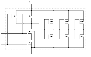
Identify at least three different transistor faults in this CMOS logic gate that could cause the output to fail low:

|
|
- �
- Transistor Q1 failed shorted (drain to source).
- �
- Transistor Q4 failed open (drain to source).
- �
- Transistor Q5 failed open (drain to source).
- �
- Transistor Q10 failed shorted (drain to source).
Notes:
One way for students to approach this problem is to re-draw the schematic in gate symbol form, a NAND gate followed by three inverters:
|
|
Discuss with them why this approach may be helpful in determining possible component faults in the integrated circuit.
Question 19:
A student builds the following circuit to demonstrate the behavior of a NAND gate:
|
|
When the student tests the circuit, though, something is wrong:
- �
- Both switches LOW, no light.
- �
- One switch HIGH, the other switch LOW; LED lights up.
- �
- One switch LOW, the other switch HIGH; LED lights up.
- �
- Both switches HIGH, no light.
Instead of acting as a NAND gate should, it seems to behave as if it were an Exclusive-OR gate! Examining the circuit for mistakes, the student discovers missing power connections to the chip - in other words, neither VDD nor VSS are connected to the power source.
While this certainly is a problem, the student is left to wonder, "How did the circuit ever function at all?" With no power connected to the chip, how is it possible that the LED ever lit in any condition?
Notes:
As an instructor of electronics, I've seen students make this mistake countless times. What is particularly troublesome about this error is the seemingly intermittent behavior of the chip. Without power supplied to the chip, most students assume there would be no function at all. So when they see the chip functioning adequately in some of its circuit's states, they are inclined to assume power is not an issue!
Question 20:
What does it mean if you see a logic gate symbol in a schematic diagram with a strange-looking "S" figure drawn inside of it?

|
|
Notes:
Schmitt trigger gates are indispensable for certain logic circuit applications. It is important that students recognize their function and utility.
Incidentally, this question provides a good opportunity to review magnetic hysteresis curves, since it's probably been awhile since students last studied electromagnetism theory!
Question 21:
In CMOS circuitry, one side of the DC power supply is usually labeled as "VDD", while the other side is labeled as "VSS". Why is this? What do the subscripts "DD" and "SS" represent?
Follow-up question: what polarities do these respective labels represent?
Notes:
Ahhh, the vestiges of yesterday's technology! What can I say? Sometimes terms ßtick" even when it makes little sense for them to.
Question 22:
A very important concept to understand in digital circuitry is the difference between current sourcing and current sinking. For instance, examine this CMOS inverting buffer gate circuit, connected to a load:
|
|
Is this gate circuit configured to source load current, sink load current, or do both?
Follow-up question: re-draw the circuit to show the gate sourcing current to an LED load.
Notes:
This very important concept is best understood from the perspective of conventional current flow notation. The terms seem backward when electron flow notation is used to track current through the output transistor.
One point of confusion I've experienced among students is that current may go either direction (in or out) of a gate with totem-pole output transistors (able to sink or source current). Some students seem to have a conceptual difficulty with current going in to the output terminal of a gate circuit, because they mistakenly associate the öut" in output as being a reference to direction of current, rather than direction of information or data.
An analogy I've used to help students overcome this problem is that of two people carrying a long pole:
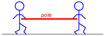
|
|
Suppose these people are in a dark, noisy room, and they use the pole as a means of simple communication between them. For example, one person could tug on the pole to get the other person's attention. Perhaps they could even develop a simple code system for communicating thoughts (1 tug = hello ; 2 tugs = good-bye ; 3 tugs = I think this is a silly way to communicate ; 4 tugs = let's leave this room ; etc.). If one of the persons pushes on the pole rather than pulls on the pole to get the other person's attention, does the direction of the pole's motion change the direction of the communication between the two persons? Of course not. Well, then, does the direction of current through the output terminal of a gate change the direction that information flows between two interconnected gates? Whether a gate sources current or sinks current to a load has no bearing on the öutput" designation of that gate terminal. Either way, the gate is still "telling the load what to do" by exercising control over the load current.
Question 23:
Suppose that a CMOS inverting buffer gate were to drive a predominantly inductive load, such as a small relay coil:
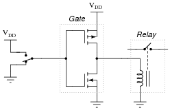
|
|
Normally, it would be considered good design practice to connect a commutating diode in parallel with the relay coil, to prevent high-voltage transients when the coil is de-energized. However, this is not necessary when a CMOS gate drives a coil. Explain why.
The correct answer has to do with the bilateral (non polarity-sensitive) nature of MOSFETs when conducting. Trace the direction of current through the relay coil while energized, and at the point in time when the gate output switches to a "low" state, and you will understand why no commutating diode is necessary in this circuit.
Notes:
By examining one of the ancillary benefits of using CMOS instead of TTL, students get a good review of inductor and transistor theory. Ask your students to explain why a TTL gate would require the relay coil to have a commutating diode, lest the gate be destroyed by inductive "kickback."
Question 24:
A problem unique to certain types of CMOS logic gates is something called SCR latchup. This is an abnormal condition capable of ruining a circuit, or at the very least causing operational problems in a circuit. Explain what this phenomenon is, and what causes it.
Challenge question: referencing a cross-sectional illustration of a CMOS gate integrated circuit, show the "SCR" formed by the transistors, and explain how it may be "fired" by excessive input voltage to the gate.
Notes:
Based on their knowledge of thyristors, your students should be able to tell you how to best ünlatch" a CMOS gate stuck in this condition. Challenge them with this problem, and also with the question of how one might detect such a condition as it's happening.
Mention to your students that not all CMOS families exhibit this problem, and that manufacturers have been keen to address serious design faults such as these. If nothing else, though, this should reinforce the lesson that one should never exceed the supply rail voltage for any type of active circuit, be it an op-amp, gate, or something else, unless expressly permitted by the manufacturer.
Question 25:
What logic state does a floating CMOS gate input naturally assume? How does this compare against traditional TTL?
Follow-up question: what state does a floating input assume for a high-speed CMOS (74HCxx) logic gate, which is designed to be an upgrade/replacement for traditional TTL gates?
Notes:
Ask your students to explain their answer based on an analysis of the internals of a CMOS gate, versus the internals of a TTL gate. Memorization is not good enough - students must grasp why these different logic families behave as they do.
Question 26:
As an electronics instructor, I have the opportunity to see a lot of creative mistakes made by students as they learn to build circuits. One very common mistake made in CMOS circuit construction manifests itself in erratic behavior: the circuit may function correctly for a time, but suddenly and randomly it stops. Then, just by waving your hand next to the circuit, it begins to work again!
This problem is especially prevalent on days where the atmospheric humidity is low, and static electric charges easily accumulate on objects and people. Explain what sort of CMOS wiring mistake would cause a powered logic gate to behave erratically due to nearby static electric fields, and what the proper solution is to this problem.
Notes:
Students think I'm a wizard by being able to troubleshoot their CMOS circuits just by waving my hand next to them. No, I'm just wise in the ways of common student error!
Question 27:
Logic probes are useful tools for troubleshooting digital logic gate circuits, but they certainly have limitations. For instance, in this simple circuit, a logic probe will give correct "high" and "low" readings at test point 1 (TP1), but it will always read "low" (even when the LED is on) at test point 2 (TP2):
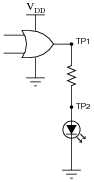
|
|
Now, obviously the output of the gate is "high" when the LED is on, otherwise it would not receive enough voltage to illuminate. Why then does a logic probe fail to indicate a high logic state at TP2?
Follow-up question: this LED circuit is rather simple, and the scenario almost silly, because the LED's presence makes checking the logic state at TP1 and TP2 superfluous! Can you think of any other circuit or situation where a similar false reading may be displayed by a logic probe - where the logic state has not been made visually obvious by the presence of an LED?
Notes:
It is easy for students to overlook the limitations of a logic probe, and to forget what actually drives it to say "high" or "low" when measuring a logic level. This is why in low-speed circuits I prefer to use a good digital voltmeter rather than a logic probe to discern logic states. With a voltmeter, you can see exactly what the voltage level is, and determine whether or not the logic state is marginal.