Differential transistor amplifiers
Question 1:
| Don't just sit there! Build something!! |
Learning to mathematically analyze circuits requires much study and practice. Typically, students practice by working through lots of sample problems and checking their answers against those provided by the textbook or the instructor. While this is good, there is a much better way.
You will learn much more by actually building and analyzing real circuits, letting your test equipment provide the änswers" instead of a book or another person. For successful circuit-building exercises, follow these steps:
- 1.
- Carefully measure and record all component values prior to circuit construction, choosing resistor values high enough to make damage to any active components unlikely.
- 2.
- Draw the schematic diagram for the circuit to be analyzed.
- 3.
- Carefully build this circuit on a breadboard or other convenient medium.
- 4.
- Check the accuracy of the circuit's construction, following each wire to each connection point, and verifying these elements one-by-one on the diagram.
- 5.
- Mathematically analyze the circuit, solving for all voltage and current values.
- 6.
- Carefully measure all voltages and currents, to verify the accuracy of your analysis.
- 7.
- If there are any substantial errors (greater than a few percent), carefully check your circuit's construction against the diagram, then carefully re-calculate the values and re-measure.
When students are first learning about semiconductor devices, and are most likely to damage them by making improper connections in their circuits, I recommend they experiment with large, high-wattage components (1N4001 rectifying diodes, TO-220 or TO-3 case power transistors, etc.), and using dry-cell battery power sources rather than a benchtop power supply. This decreases the likelihood of component damage.
As usual, avoid very high and very low resistor values, to avoid measurement errors caused by meter "loading" (on the high end) and to avoid transistor burnout (on the low end). I recommend resistors between 1 kW and 100 kW.
One way you can save time and reduce the possibility of error is to begin with a very simple circuit and incrementally add components to increase its complexity after each analysis, rather than building a whole new circuit for each practice problem. Another time-saving technique is to re-use the same components in a variety of different circuit configurations. This way, you won't have to measure any component's value more than once.
Notes:
It has been my experience that students require much practice with circuit analysis to become proficient. To this end, instructors usually provide their students with lots of practice problems to work through, and provide answers for students to check their work against. While this approach makes students proficient in circuit theory, it fails to fully educate them.
Students don't just need mathematical practice. They also need real, hands-on practice building circuits and using test equipment. So, I suggest the following alternative approach: students should build their own "practice problems" with real components, and try to mathematically predict the various voltage and current values. This way, the mathematical theory "comes alive," and students gain practical proficiency they wouldn't gain merely by solving equations.
Another reason for following this method of practice is to teach students scientific method: the process of testing a hypothesis (in this case, mathematical predictions) by performing a real experiment. Students will also develop real troubleshooting skills as they occasionally make circuit construction errors.
Spend a few moments of time with your class to review some of the "rules" for building circuits before they begin. Discuss these issues with your students in the same Socratic manner you would normally discuss the worksheet questions, rather than simply telling them what they should and should not do. I never cease to be amazed at how poorly students grasp instructions when presented in a typical lecture (instructor monologue) format!
A note to those instructors who may complain about the "wasted" time required to have students build real circuits instead of just mathematically analyzing theoretical circuits:
What is the purpose of students taking your course?
If your students will be working with real circuits, then they should learn on real circuits whenever possible. If your goal is to educate theoretical physicists, then stick with abstract analysis, by all means! But most of us plan for our students to do something in the real world with the education we give them. The "wasted" time spent building real circuits will pay huge dividends when it comes time for them to apply their knowledge to practical problems.
Furthermore, having students build their own practice problems teaches them how to perform primary research, thus empowering them to continue their electrical/electronics education autonomously.
In most sciences, realistic experiments are much more difficult and expensive to set up than electrical circuits. Nuclear physics, biology, geology, and chemistry professors would just love to be able to have their students apply advanced mathematics to real experiments posing no safety hazard and costing less than a textbook. They can't, but you can. Exploit the convenience inherent to your science, and get those students of yours practicing their math on lots of real circuits!
Question 2:
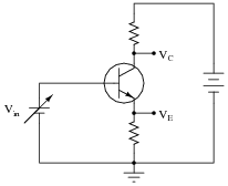
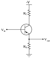
A qualitative model for transistor behavior is that of a variable resistor. While grossly inaccurate in a quantitative (numbers) sense, it at least provides a means of assessing its behavior in the sense of "more conductive" or "less conductive".
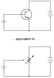
|
|
Apply this "model" of transistor behavior to this single-transistor amplifier circuit, and describe what happens to the collector voltage (VC) and emitter voltage (VE) when the input voltage (Vin) increases and decreases:
|
|
Notes:
If this concept is confusing to any of your students, draw a pair of three-resistor voltage divider circuits on the whiteboard for everyone to see, and then have the students analyze the voltage drops in two conditions: when the middle resistor is a low value, and when the middle resistor is a high value.
Astute students will recognize this transistor circuit configuration as a phase splitter.
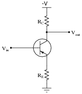
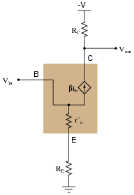
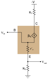
Question 3:
Identify the type of transistor amplifier this is (common-collector, common-emitter, or common-base), and identify whether it is inverting or noninverting.
|
|
Also, explain how to derive the voltage gain equation for this amplifier:
|
|
|
Follow-up question: the voltage gain equation for this type of transistor amplifier is usually shown in a simpler form that what I provided at the end of the question. Write this simpler form, and explain why it is approximately true.
Notes:
In discussion with your students, analyze the response of this single-transistor amplifier circuit for a variety of input voltages. In other words, perform a thought experiment to re-familiarize them with the behavior of this transistor amplifier configuration. Plot the input and output voltages, if necessary, on a graph. Discuss what the term ïnverting" means in this context.
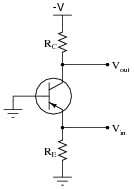
Question 4:
Identify the type of transistor amplifier this is (common-collector, common-emitter, or common-base), and identify whether it is inverting or noninverting.
|
|
Also, explain how to derive the voltage gain equation for this amplifier:
|
|
|
Follow-up question: the voltage gain equation for this type of transistor amplifier is usually shown in a simpler form that what I provided at the end of the question. Write this simpler form, and explain why it is approximately true.
Notes:
In discussion with your students, analyze the response of this single-transistor amplifier circuit for a variety of input voltages. In other words, perform a thought experiment to re-familiarize them with the behavior of this transistor amplifier configuration. Plot the input and output voltages, if necessary, on a graph. Discuss what the term "noninverting" means in this context.
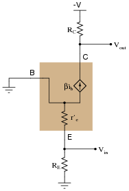
Question 5:
Identify the type of transistor amplifier this is (common-collector, common-emitter, or common-base), and identify whether it is inverting or noninverting.
|
|
Also, explain how to derive the voltage gain equation for this amplifier:
|
|
|
Notes:
In discussion with your students, analyze the response of this single-transistor amplifier circuit for a variety of input voltages. In other words, perform a thought experiment to re-familiarize them with the behavior of this transistor amplifier configuration. Plot the input and output voltages, if necessary, on a graph. Discuss what the term "noninverting" means in this context.
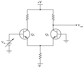
Question 6:
Would you characterize this transistor amplifier as being inverting or noninverting, with the base terminal of transistor Q2 being considered the input? Explain your answer.
|
|
Notes:
Ask your students to remove transistor Q1 (and its collector resistor) from the circuit and try answering the question then. It should be easy to determine whether the circuit is inverting or noninverting in that configuration. Then, have your students ïnsert" Q1 and its collector resistor back into the circuit and re-analyze. Does the presence of Q1 change anything? Why or why not?
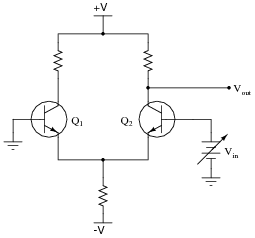
Question 7:
Would you characterize this transistor amplifier as being inverting or noninverting, with the base terminal of transistor Q1 being considered the input? Explain your answer.
|
|
Follow-up question: what happens to the collector-emitter conductivity of transistor Q2 as transistor Q1 passes more current due to an increasing Vin signal?
Notes:
Analysis of this circuit is aided by applying the "variable resistor" model of the transistor to it. Substitute variable resistors for the transistors Q1 and Q2, and then have your students analyze it as a voltage divider circuit.
The follow-up question is important because it implies transistor Q2 is not a static entity with changes in Q1's base signal. The same may be said for Q1 when changes occur at the base of Q2. Discuss this effect with your students, making sure they understand why both transistors' conductivity changes with a change in only one of the base voltages.
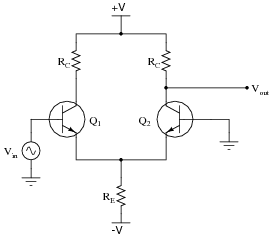
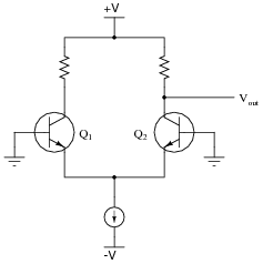
Question 8:
Here, a differential pair circuit is driven by an input voltage at the base of Q2, while the output is taken at the collector of Q2. Meanwhile, the other input (Q1 base) is connected to ground:
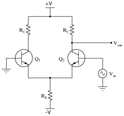
|
|
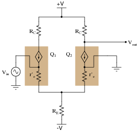
Identify what types of amplifier circuits the two transistors are functioning as (common-collector, common-emitter, common-base) when the differential pair is used like this, and write an equation describing the circuit's voltage gain. Here is another schematic, showing the transistors modeled as controlled current sources, to help you with the equation:
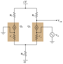
|
|
|
Follow-up question #1: explain why it is appropriate to simplify the gain equation to this:
|
Follow-up question #2: explain why the simplified gain equation is sometimes written with a negative sign in it:
|
Notes:
The purpose of this question is to have students analyze the resistances in the differential pair circuit to develop their own gain equation, based on their understanding of how simpler transistor amplifier circuit gains are derived. Ultimately, this question should lead into another one asking students to express the differential voltage gain of the circuit (a superposition of the gain equations for each input considered separately).
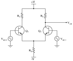
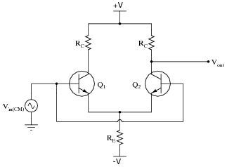
Question 9:
Here, a differential pair circuit is driven by an input voltage at the base of Q1, while the output is taken at the collector of Q2. Meanwhile, the other input (Q2 base) is connected to ground:
|
|
Identify what types of amplifier circuits the two transistors are functioning as (common-collector, common-emitter, common-base) when the differential pair is used like this, and write an equation describing the circuit's voltage gain. Here is another schematic, showing the transistors modeled as controlled current sources, to help you with the equation:
|
|
|
Follow-up question: explain why it is appropriate to simplify the gain equation to this:
|
Notes:
The purpose of this question is to have students analyze the resistances in the differential pair circuit to develop their own gain equation, based on their understanding of how simpler transistor amplifier circuit gains are derived. Ultimately, this question should lead into another one asking students to express the differential voltage gain of the circuit (a superposition of the gain equations for each input considered separately).
Admittedly, the unsimplified equation shown in the answer is daunting, and students may wonder where I got it. You may help them understand that the basic gain equation for a BJT amplifier is founded on the assumption that IC � IE, that any current through the emitter terminal will be "repeated" at the collector terminal to flow through the collector resistance. Thus, voltage gain is nothing more than a ratio of resistances, given that emitter current and collector current are assumed to be the same:
|
|
|
Thus, deriving a gain equation for a BJT amplifier is usually as simple as figuring out what resistance the collector current goes through and dividing that by the amount of resistance the base-to-emitter current has to go through. In a grounded-base amplifier, this ratio is simply [(RC)/(r�e)].
With this circuit, however, the input signal must fight its way through the r�e of Q1 before ever getting to Q2 to be amplified, which is why the voltage gain equation is so much more complex. After going through the dynamic emitter resistance of Q1, it splits between the dynamic emitter resistance of Q2 and the "tail" resistance RE. The term r�e + (r�e || RE) is the amount of resistance the AC input signal travels through, and the fraction [(r�e || RE)/(r�e)] defines the splitting of current (most to the emitter of Q2, a small amount through RE).
Question 10:
Write an approximate equation describing the differential voltage gain for a differential pair circuit such as this, in terms of the component values:
|
|
|
Follow-up question: what component value(s) should be altered to maximize differential voltage gain in a differential pair circuit, and why?
Notes:
The purpose of this question is to have students apply the Superposition theorem to combine two voltage gain equations into a single differential voltage gain equation.
Question 11:
Describe what happens to each of the output voltages (Vout1 and Vout2) as the input voltage (Vin) decreases:

|
|
Notes:
With four terminals to connect to the outside world, this circuit is a differential-input, differential-output amplifier.
Question 12:
Suppose this differential-pair circuit was perfectly balanced. In this condition, how much voltage would be expected between the two transistors' collector terminals?
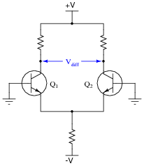
|
|
What would happen to this differential voltage (Vdiff) if transistor Q2 were to increase in temperature, while transistor Q1 remained at the same temperature? Explain your answer.
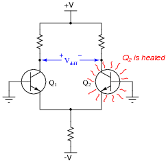
|
|
Follow-up question: what does this phenomenon mean with regard to the stability of differential-pair transistor circuits under different operating conditions? What might be a good way to maximize circuit stability over a wide range of operating temperatures?
Notes:
Fundamentally, the issue in this question is what happens to a transistor when it heats up, but the electrical supply (power and input signal) parameters do not change. Ask your students to relate this phenomenon to the behavior of other PN junction devices, such as diodes.
Question 13:
This circuit is part of a weather monitoring station. Wind speed is measured by the voltage output from a permanent-magnet DC generator, turned by a set of vanes. A light bulb lights up when the wind speed passes a threshold ("trip") value, established by the potentiometer:
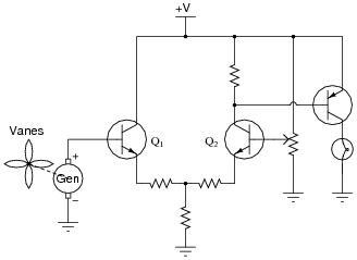
|
|
Based on your understanding of differential pair circuits, is this a high-speed wind indicating circuit or a low-speed wind indicating circuit?
Notes:
Ask your students to explain their reasoning in obtaining their answers. What happens in this circuit as the generator voltage increases, and as it decreases? Which way do we adjust the potentiometer to increase the trip point? How do we know this?
Let your students know that this circuit is a simple example of what is called a comparator: a circuit that compares two voltages against each other and generates an output corresponding to which voltage is greater.
Question 14:
What is common-mode voltage, and how should a differential amplifier (ideally) respond to it?
Follow-up question: what does the phrase common-mode rejection ratio (CMRR) mean for a differential amplifier?
Notes:
Ask your students to provide examples of common-mode voltage to a differential amplifier. For example, x amount of voltage on one input and y amount of voltage on the other constitutes z amount of common-mode voltage . . .
Question 15:
If we connect the two transistor bases together in a differential pair circuit, it can only see common-mode input voltage (no differential input voltage):
|
|
An important performance parameter of any differential amplifier is its common-mode voltage gain. Ideally, a differential-input amplifier should ignore any and all common-mode voltage, but in reality there is always some amplification of common-mode voltage. We need to figure out how much of that there will be in any differential-pair circuit.
To help us analyze this circuit (with both inputs tied together so it only sees common-mode input voltage), I will re-draw it in such a way that reflects the symmetrical nature of the circuit:
|
|
First, explain why this re-drawing is justified, and then write the equation describing the common-mode voltage gain of this circuit, in terms of the component values.
Re-drawn like this, it should be plain to see that the differential pair acts as a swamped common-emitter amplifier, with the common-mode voltage gain described by the following equation:
|
Follow-up question: what component value(s) should be altered to minimize common-mode voltage gain in a differential pair circuit, and why?
Notes:
The purpose of this question is to have students recognize what factors in a differential pair circuit influence common-mode voltage gain, and then to realize that the value of the tail resistor has great influence over common-mode gain, while at the same time having negligible influence over differential gain.
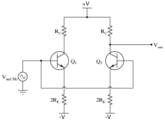
Question 16:
An improvement to the resistor-based differential amplifier design is the addition of a constant-current source where the two transistors' emitter currents mesh together:
|
|
What does the constant-current source "look like" to the rest of the amplifier, in terms of equivalent resistance? What advantage does this give to the amplifier's performance, over the (simpler) resistor design? Finally, how is this constant-current source actually constructed in a typical differential amplifier circuit?
Notes:
Ask your students to define CMRR and explain its importance in a differential amplifier circuit. Analyze the effects of common-mode input voltage on a simple resistor-based differential amplifier circuit, and then compare it to the circuit having a constant current source. How does the current source work to improve CMRR (reduce common-mode gain)?
Also, have your students draw a current mirror for this differential amplifier circuit and explain how it works.
I am expecting that your students have seen (or can research) the CMRR approximation for a differential pair circuit (CMRR � [(RE)/(r�e)]), and from this can deduce the importance of using a current source in the tail of the circuit instead of a passive resistor.
Question 17:
Common-mode rejection ratio is the ratio between a differential amplifier's differential voltage gain and its common-mode voltage gain:
|
The greater this parameter's value, the better the differential amplifier will perform as a truly differential amplifier. Combine the equations for differential voltage gain and for common-mode voltage gain for the following differential amplifier circuit, into a single equation for CMRR:

|
|
|
Follow-up question: what component value(s) should be altered to maximize CMRR in a differential pair circuit, and why?
Notes:
You might want to add that CMRR is usually expressed in decibels, calculated the same way you would calculate decibels for any other ratio of voltages.
Question 18:
Differential amplifiers often make use of active loads: a current mirror circuit to establish collector currents between the two transistors, rather than load resistors.
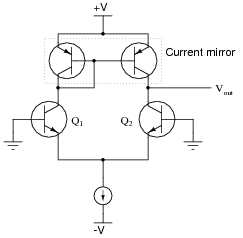
|
|
What does the current mirror "look like" to the common-emitter side of the differential amplifier circuit, when we apply the Superposition theorem? What aspect of the differential amplifier's performance is primarily enhanced with the addition of the current mirror to the circuit?
Notes:
Ask your students to explain why the differential voltage gain increases. One hint is the internal (Norton) resistance of an ideal current source: infinite ohms! Ask your students how this equivalent resistance compares to the (finite) values of the resistors replaced by the current mirror, and what impact that change has on voltage gain.
Question 19:
Predict how the operation of this differential pair circuit will be affected as a result of the following faults. Consider each fault independently (i.e. one at a time, no multiple faults):
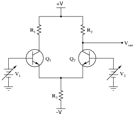
|
|
- �
- Resistor R1 fails open:
- �
- Resistor R2 fails open:
- �
- Resistor R3 fails open:
- �
- Solder bridge (short) across resistor R3:
For each of these conditions, explain why the resulting effects will occur.
- �
- Resistor R1 fails open: More current will be drawn from V1; if V1 sags as a result, Vout will decrease.
- �
- Resistor R2 fails open: Vout will assume a voltage level approximately equal to V2 - 0.7 volts.
- �
- Resistor R3 fails open: Vout saturates to +V (positive supply rail).
- �
- Solder bridge (short) across resistor R3: Vout saturates to within a few tenths of a volt from -V (negative supply rail).
Notes:
The purpose of this question is to approach the domain of circuit troubleshooting from a perspective of knowing what the fault is, rather than only knowing what the symptoms are. Although this is not necessarily a realistic perspective, it helps students build the foundational knowledge necessary to diagnose a faulted circuit from empirical data. Questions such as this should be followed (eventually) by other questions asking students to identify likely faults based on measurements.