Junction field-effect transistors
Question 1:
| Don't just sit there! Build something!! |
Learning to mathematically analyze circuits requires much study and practice. Typically, students practice by working through lots of sample problems and checking their answers against those provided by the textbook or the instructor. While this is good, there is a much better way.
You will learn much more by actually building and analyzing real circuits, letting your test equipment provide the änswers" instead of a book or another person. For successful circuit-building exercises, follow these steps:
- 1.
- Carefully measure and record all component values prior to circuit construction, choosing resistor values high enough to make damage to any active components unlikely.
- 2.
- Draw the schematic diagram for the circuit to be analyzed.
- 3.
- Carefully build this circuit on a breadboard or other convenient medium.
- 4.
- Check the accuracy of the circuit's construction, following each wire to each connection point, and verifying these elements one-by-one on the diagram.
- 5.
- Mathematically analyze the circuit, solving for all voltage and current values.
- 6.
- Carefully measure all voltages and currents, to verify the accuracy of your analysis.
- 7.
- If there are any substantial errors (greater than a few percent), carefully check your circuit's construction against the diagram, then carefully re-calculate the values and re-measure.
When students are first learning about semiconductor devices, and are most likely to damage them by making improper connections in their circuits, I recommend they experiment with large, high-wattage components (1N4001 rectifying diodes, TO-220 or TO-3 case power transistors, etc.), and using dry-cell battery power sources rather than a benchtop power supply. This decreases the likelihood of component damage.
As usual, avoid very high and very low resistor values, to avoid measurement errors caused by meter "loading" (on the high end) and to avoid transistor burnout (on the low end). I recommend resistors between 1 kW and 100 kW.
One way you can save time and reduce the possibility of error is to begin with a very simple circuit and incrementally add components to increase its complexity after each analysis, rather than building a whole new circuit for each practice problem. Another time-saving technique is to re-use the same components in a variety of different circuit configurations. This way, you won't have to measure any component's value more than once.
Notes:
It has been my experience that students require much practice with circuit analysis to become proficient. To this end, instructors usually provide their students with lots of practice problems to work through, and provide answers for students to check their work against. While this approach makes students proficient in circuit theory, it fails to fully educate them.
Students don't just need mathematical practice. They also need real, hands-on practice building circuits and using test equipment. So, I suggest the following alternative approach: students should build their own "practice problems" with real components, and try to mathematically predict the various voltage and current values. This way, the mathematical theory "comes alive," and students gain practical proficiency they wouldn't gain merely by solving equations.
Another reason for following this method of practice is to teach students scientific method: the process of testing a hypothesis (in this case, mathematical predictions) by performing a real experiment. Students will also develop real troubleshooting skills as they occasionally make circuit construction errors.
Spend a few moments of time with your class to review some of the "rules" for building circuits before they begin. Discuss these issues with your students in the same Socratic manner you would normally discuss the worksheet questions, rather than simply telling them what they should and should not do. I never cease to be amazed at how poorly students grasp instructions when presented in a typical lecture (instructor monologue) format!
A note to those instructors who may complain about the "wasted" time required to have students build real circuits instead of just mathematically analyzing theoretical circuits:
What is the purpose of students taking your course?
If your students will be working with real circuits, then they should learn on real circuits whenever possible. If your goal is to educate theoretical physicists, then stick with abstract analysis, by all means! But most of us plan for our students to do something in the real world with the education we give them. The "wasted" time spent building real circuits will pay huge dividends when it comes time for them to apply their knowledge to practical problems.
Furthermore, having students build their own practice problems teaches them how to perform primary research, thus empowering them to continue their electrical/electronics education autonomously.
In most sciences, realistic experiments are much more difficult and expensive to set up than electrical circuits. Nuclear physics, biology, geology, and chemistry professors would just love to be able to have their students apply advanced mathematics to real experiments posing no safety hazard and costing less than a textbook. They can't, but you can. Exploit the convenience inherent to your science, and get those students of yours practicing their math on lots of real circuits!
Question 2:
Field effect transistors are classified as majority carrier devices. Explain why.
Review question: in contrast, why are bipolar junction transistors considered minority carrier devices?
Notes:
Ask your students what type of transistor operates on a minority carrier principle, as opposed to field-effect transistors.
Question 3:
What does the term transconductance mean, with reference to a field-effect transistor? Is the transconductance function for an FET a linear or a nonlinear relationship? Explain why, making reference to an equation if at all possible to explain your answer.
Challenge question: what unit of measurement would be appropriate for expressing transconductance in?
Notes:
Transconductance is not just a parameter for JFETs, but also MOSFETs (IGFETs) and vacuum tubes. Any voltage-controlled current-regulating device has a transconductance value (though it may change over the operating range of the device, just as b changes over the operating range of a BJT).
Question 4:
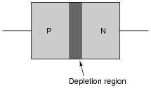
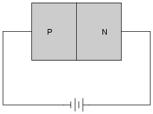
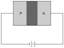
The dark shaded area drawn in this cross-section of a PN junction represents the depletion region:
|
|
Re-draw the depletion region when the PN junction is subjected to a reverse-bias voltage:
|
|
|
|
Follow-up questions: describe the conductivity of the depletion region: is it high or low? What exactly does the word "depletion" refer to, anyway?
Notes:
This question makes a good lead-in to a discussion of JFET operation, where the channel conductivity is modulated by the width of the gate-channel depletion region.
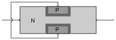
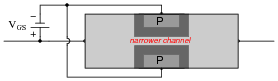
Question 5:
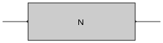
A field-effect transistor is made from a continuous "channel" of doped semiconductor material, either N or P type. In the illustration shown below, the channel is N-type:
|
|
Trace the direction of current through the channel if a voltage is applied across the length as shown in the next illustration. Determine what type of charge carriers (electrons or holes) constitute the majority of the channel current:
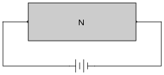
|
|
The next step in the fabrication of a field-effect transistor is to implant regions of oppositely-doped semiconductor on either side of the channel as shown in the next illustration. These two regions are connected together by wire, and called the "gate" of the transistor:
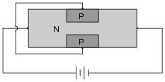
|
|
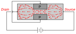
Show how the presence of these "gate" regions in the channel influence the flow of charge carriers. Use small arrows if necessary to show how the charge carriers move through the channel and past the gate regions of the transistor. Finally, label which terminal of the transistor is the source and which terminal is the drain, based on the type of majority charge carrier present in the channel and the direction of those charge carriers' motion.
|
|
This makes the right-hand terminal the source and the left-hand terminal the drain.
Follow-up question: explain why the charge carriers avoid traversing the PN junctions formed by the gate-channel interfaces. In other words, explain why we do not see this happening:
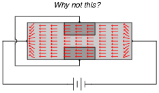
|
|
Notes:
Students typically find junction field-effect transistors much easier to understand than bipolar junction transistors, because there is less understanding of energy levels required to grasp the operation of JFETs than what is required to comprehend the operation of BJTs. Still, students need to understand how different charge carriers move through N- and P-type semiconductors, and what the significance of a depletion region is.
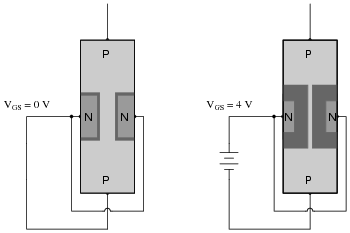
Question 6:
Field-effect transistors (FETs) exhibit depletion regions between the oppositely-doped gate and channel sections, just as diodes have depletion regions between the P and N semiconductor halves. In this illustration, the depletion region appears as a dark, shaded area:
|
|
Re-draw the depletion regions for the following scenarios, where an external voltage (VGS) is applied between the gate and channel:
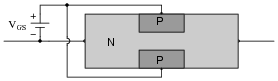
|
|
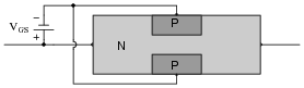
|
|
Note how the different depletion region sizes affect the conductivity of the transistor's channel.
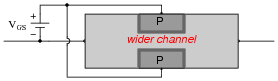
|
|
|
|
Follow-up question: why do you suppose this type of transistor is called a field-effect transistor? What "field" is being referred to in the operation of this device?
Notes:
The effect that this external gate voltage has on the effective width of the channel should be obvious, leading students to understand how a JFET allows one signal to exert control over another (the basic principle of any transistor, field-effect or bipolar).
Question 7:
Bipolar junction transistors (BJTs) are considered "normally-off" devices, because their natural state with no signal applied to the base is no conduction between emitter and collector, like an open switch. Are junction field-effect transistors (JFETs) considered the same? Why or why not?
Notes:
Ask your students to elaborate on the answer given. Do not accept a mindless recitation of the answer, "JFETs are normally-on devices," but rather demand that some sort of explanation be given as to why JFETs are normally-on devices.
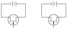
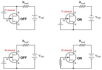
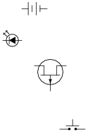
Question 8:
Match the following field-effect transistor illustrations to their respective schematic symbols:
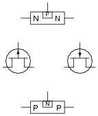
|
|
|
|
Notes:
Be sure to ask your students to identify which symbol is the "P-channel" and which is the "N-channel" transistor!
It might help to review diode symbols, if some students experience difficulty in matching the designations (P-channel versus N-channel) with the schematic symbols.
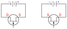
Question 9:
Based on these DC continuity tester indications, what type of JFET is this, N-channel or P-channel?
- �
- Resistance with negative test lead on pin 1, positive test lead on pin 2: no continuity
- �
- Resistance with negative test lead on pin 1, positive test lead on pin 3: no continuity
- �
- Resistance with negative test lead on pin 2, positive test lead on pin 1: continuity
- �
- Resistance with negative test lead on pin 2, positive test lead on pin 3: continuity
- �
- Resistance with negative test lead on pin 3, positive test lead on pin 1: continuity
- �
- Resistance with negative test lead on pin 3, positive test lead on pin 2: continuity
Also, to the best of your ability, identify the transistor's three terminals (source, gate, and drain).
Notes:
Advise your students about the risks of using an analog multimeter (in ohmmeter mode) to test semiconductor components. Some inexpensive analog multimeter designs actually switch the polarity of the test leads when in the ohmmeter mode. In other words, the red test lead actually connects to the negative side of the meter's internal battery, while the black test lead connects to the positive side of the internal battery! If you are used to associating red with positive and black with negative, this switch will be quite a surprise.
Ask your students: what effect would a switch in polarity such as the one just described have on the determination of a transistor's identity? What if the person thought their meter's red lead was positive and the black lead negative, when in fact it was just the opposite? Would this affect their ability to accurately identify the transistor's terminals? Why or why not?
Question 10:
From the "diode check" measurements taken with these two meters, identify the terminals on this JFET, and also what type of JFET it is (N-channel or P-channel):
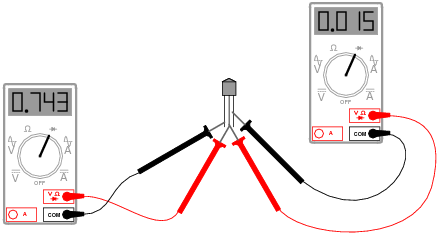
|
|
Notes:
Ask your students to explain why the gate-channel junction registers a voltage drop of 0.743 volts, while the source-drain path only registers 15 millivolts of drop. What does this indicate about the conductivity of JFET compared to that of a BJT? Also, what does this suggest about the minimum source-drain voltage necessary for controlled current to go through the JFET?
Question 11:
Identify which transistor terminal functions as the source and which transistor terminal functions as the drain in both of these JFET circuits:
|
|
Most importantly, explain why we define the terminals as such, given the fact that is usually no physical difference between these two terminals of a JFET.
|
|
The "why" answer is related to the type of majority charge carrier within the channel of each JFET.
Notes:
The distinction between source and drain for any kind of FET (JFET or MOSFET) is important because the controlling voltage (VGS) must be applied between gate and source, not between gate and drain.
Question 12:
Junction field-effect transistors (JFETs) are normally-on devices, the natural state of their channels being passable to electric currents. Thus, a state of cutoff will only occur on command from an external source.
Explain what must be done to a JFET, specifically, to drive it into a state of cutoff.
Follow-up question: is any gate current required to drive a JFET into the cutoff state? Why or why not?
Notes:
This is perhaps the most important question your students could learn to answer when first studying JFETs. What, exactly, is necessary to turn one off? Have your students draw diagrams to illustrate their answers as they present in front of the class.
Question 13:
Explain what cutoff voltage (VGS(off)) is for a field-effect transistor. Research the datasheets for some of the following field-effect transistors and determine what their respective cutoff voltages are:
- �
- J110
- �
- J308
- �
- J309
- �
- J310
- �
- MPF 102
Follow-up question: based on your research of these datasheets, how constant is VGS(off) between different transistors? In other words, is this a parameter you can accurately predict from the datasheet before purchasing a transistor, or does it vary significantly from transistor to transistor (of the same part number)?
Notes:
Discuss with your students the significance of VGS(off), especially its stability (or instability, as the case may be) between transistors. How does this impact the design of FET circuits?
Question 14:
The equation solving for drain current through a JFET is as follows:
|
Where,
ID = Drain current
IDSS = Drain current with the Gate terminal shorted to the Source terminal
VGS = Applied Gate-to-Source voltage
VGS(off) = Gate-to-Source voltage necessary to "cut off" the JFET
Algebraically manipulate this equation to solve for VGS, and explain why this new equation might be useful to us.
|
Notes:
This question is primarily an exercise in algebraic manipulation. Have your students show their work in front of the class, to show others the strategy involved to manipulate such an equation.
Question 15:
The power dissipation of a JFET may be calculated by the following formula:
|
For all practical purposes, though, this formula may be simplified and re-written as follows:
|
Explain why the second term of the original equation (VGSIG) may be safely ignored for a junction field-effect transistor.
Notes:
This question asks students to look beyond the equation to the device itself and think about the relative magnitudes of each variable. Many equations in electronics (and other sciences!) may be similarly simplified by recognizing the relative magnitudes of variables and eliminating those whose overall effect on the equation's result will be negligible. Of course, what constitutes "negligible" will vary from context to context.
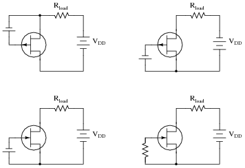
Question 16:
Identify each type of JFET (whether it is N-channel or P-channel), label the terminals, and determine whether the JFET in each of these circuits will be turned on or off:
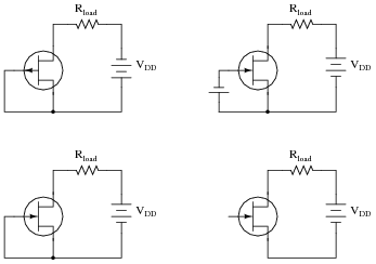
|
|
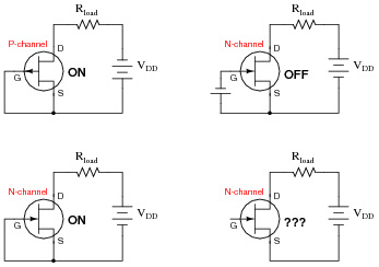
|
|
Follow-up question: explain why the lower-right circuit has question-marks next to the transistor. Why is the JFET's state uncertain?
Notes:
It is very important for your students to understand what factor(s) in a circuit force a JFET to turn on or off. Be sure to ask your students to explain their reasoning for each transistor's status. What factor, or combination of factors, is necessary to turn a JFET on, versus off? One point of this question is to emphasize the non-importance of VDD's polarity when there is an external biasing voltage applied directly between gate and source.
Question 17:
Identify each type of JFET (whether it is N-channel or P-channel), label the terminals, and determine whether the JFET in each of these circuits will be turned on or off:
|
|
Additionally, identify which of these four circuits places unnecessary stress on the transistor. There is one circuit among these four where the transistor is operated in a state that might lead to premature failure.
|
|
The upper-right circuit places unnecessary stress on the JFET.
Notes:
It is very important for your students to understand what factor(s) in a circuit force a JFET to turn on or off. Be sure to ask your students to explain their reasoning for each transistor's status. What factor, or combination of factors, is necessary to turn a JFET on, versus off? One point of this question is to emphasize the non-importance of VDD's polarity when there is an external biasing voltage applied directly between gate and source.
Discuss with your students precisely what is wrong with the upper-right JFET circuit. Why is the transistor being stressed? How do we avoid such a problem?
Question 18:
When a reverse-bias voltage is applied between the gate and channel of a JFET, the depletion region within expands. The greater the reverse-bias voltage, the wider the depletion region becomes. With enough applied VGS, this expansion will cut off the JFET's channel, preventing drain-source current:
|
|
Something not immediately apparent about this effect is that the formation of a wide depletion region necessary for cut-off of a field-effect transistor is also affected by the drain-to-source voltage drop (VDS).
|
|
If we connect a gate-to-source voltage (VGS) large enough to force the transistor into cutoff mode, the JFET channel will act as a huge resistance. If we look carefully at the voltages measured with reference to ground, we will see that the width of the depletion region must vary within the JFET's channel. Sketch this varying width, given the voltages shown in the illustration:
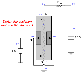
|
|
Something really interesting happens if we reverse the polarity of the 20 volt source: the relationship between drain and source changes, and so does the depletion region profile. Sketch the new varying width of the depletion region with the 20 volt source reversed, and comment on what you see:
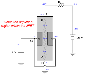
|
|
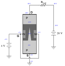
|
|
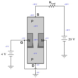
|
|
Follow-up question: you can see that the transistor doesn't even cut off as expected with the 20 volt source reversed. What would we have to do to get this JFET to cut off with a only 4 volt control signal, since having reversed the 20 volt source?
Notes:
There is more than one correct answer for the follow-up question. Discuss this with your students, emphasizing the importance of properly identifying drain and source according to VDS polarity.
Question 19:
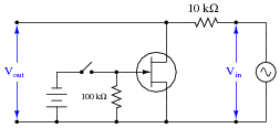
Determine what status the LED will be in (either ön" or öff") for both switch positions in this JFET switching circuit:
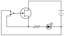
|
|
Notes:
Ask your students to explain their reasoning for their switch position determinations.
Question 20:
This circuit has an unusual problem. When the switch is open, the LED turns on. When the switch is closed, the LED turns off. However, when the switch is opened again, the LED often does not turn back on until some time has passed. Others notice that sometimes the LED will turn on and off just by waving their hand next to it, with the switch in the open position.
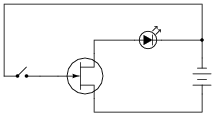
|
|
Explain what is happening here, and also propose a solution to eliminate the unpredictability when the switch is open.
Notes:
Challenge your students to place a resistor in this circuit in such a way as to meet the requirements of the given solution.
Incidentally, this circuit makes an excellent classroom demonstration for students to experiment with.
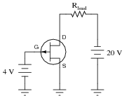
Question 21:
What is wrong with this JFET circuit? What might happen to the transistor if this circuit is built and operated?
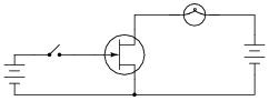
|
|
Notes:
Have your students consult a typical JFET datasheet and research the maximum gate current parameter. Discuss this parameter with your students, and also talk about how we can make sure this limitation is not exceeded in any circuit design.
The latter subject is very important for students because I have seen many a JFET destroyed by this exact type of abuse.
Question 22:
Draw the connecting wires to form a circuit where the transistor turns the LED off whenever the pushbutton switch is actuated:
|
|
|
|
Notes:
Ask your students to describe the biasing of the gate-channel junction inside the transistor when the switch is closed. Is this PN junction forward-biased, or reverse-biased? What does this biasing do inside the transistor to interrupt current to the LED?
Note that there is no resistor shown in this circuit, because many small-signal JFETs have values of IDSS within the operating range of common LEDs. In other words, the JFET itself acts as a current-limiting device to protect the LED.
Question 23:
Junction field-effect transistors are very sensitive devices, requiring practically zero current to "drive" them into either cutoff or saturation. However, they usually cannot handle high drain currents - in other words, they are not considered "power" switching devices.
If we combine a JFET with a BJT, though, we may realize the best features of each transistor: low drive current requirements combined with a high controlled current rating. Examine the following hybrid JFET/BJT circuits, and explain how each one works to control power to the load:
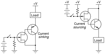
|
|
Determine for each circuit whether the load becomes energized when the switch is closed or when it is opened, and explain how each one works.
Follow-up question: explain the purpose of the resistor in each circuit. What might happen if it were not there?
Notes:
This question is a good review of both BJT and JFET operating theory, as well as a practical example of how "cascading" different types of transistors may result in "best of both worlds" performance.
Question 24:
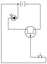
Junction field-effect transistors have the ability to perform some functions that are impossible with (single) bipolar junction transistors. Take this circuit, for example:
|
|
What effect will opening and closing the toggle switch have on the AC signal measured at the output terminals?
Notes:
Discuss how the JFET is able to perform this AC signal ßhunting" function, whereas a BJT would not be able to do the same. Can your students think of any practical applications of a circuit like this?
Question 25:
Predict how this circuit will be affected as a result of the following faults. Consider each fault independently (i.e. one at a time, no multiple faults):
|
|
- �
- Diode D1 fails open:
- �
- Transistor Q1 fails shorted (drain-to-source):
- �
- Transistor Q1 fails open (drain-to-source):
- �
- Transistor Q2 fails shorted (collector-to-emitter):
For each of these conditions, explain why the resulting effects will occur.
- �
- Diode D1 fails open: Audio signal always passes through and cannot be turned off.
- �
- Transistor Q1 fails shorted (drain-to-source): Audio signal always passes through and cannot be turned off.
- �
- Transistor Q1 fails open (drain-to-source): Audio signal never passes through and cannot be turned on.
- �
- Transistor Q2 fails shorted (collector-to-emitter): Audio signal never passes through and cannot be turned on.
Notes:
The purpose of this question is to approach the domain of circuit troubleshooting from a perspective of knowing what the fault is, rather than only knowing what the symptoms are. Although this is not necessarily a realistic perspective, it helps students build the foundational knowledge necessary to diagnose a faulted circuit from empirical data. Questions such as this should be followed (eventually) by other questions asking students to identify likely faults based on measurements.
Question 26:
Junction Field-Effect Transistors (JFETs) differ in behavior from Bipolar Junction Transistors (BJTs) in several ways. Address each one of these behavioral aspects in your answer:
- �
- Current gain
- �
- Conduction with no input (gate/base) signal
- �
- Polarization
JFETs are normally-on devices. BJTs are normally-off devices.
JFETs can pass current from source to drain, or from drain to source with equal ease. BJTs can only pass current from emitter to collector in one direction.
Notes:
For each one of these behavioral aspects, discuss with your students exactly why the two transistors types differ.
Question 27:
When measuring the resistance of a JFET from source to drain, the ohmmeter reading may be seen to change simply by touching the gate terminal with your finger:
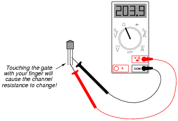
|
|
Such a degree of sensitivity is unheard of in bipolar junction transistors. Explain why the JFET is so sensitive, and comment on what advantages and disadvantages this gives the JFET as an electronic device.
Notes:
The stated answer is purposefully vague, to force students to think and to express the answer in their own words.
It is quite easy to demonstrate this sensitivity in the classroom with nothing more than an ohmmeter and a JFET, and so I encourage you to set this up as a demonstration for your students.
Question 28:
What is the proper unit of measurement for the transconductance of a field-effect transistor (or an electron tube, which exhibits similar characteristics)? Explain why this unit makes sense, based on the mathematical definition of transconductance.
Notes:
Although the physical meaning of transconductance (gm) is significantly different from the physical meaning of conductance (G), they share the same unit of measurement due to their respective mathematical definitions. Discuss the concept of dimensional analysis with your students if they have not yet been exposed to it thus far through their use of physics formulae.
Question 29:
Although field-effect transistors are not usually characterized in terms of current gain as bipolar junction transistors are, it would not be wrong to speak of FETs as having current gains. Compared to a BJT, how does the current gain of a FET compare? Explain your answer.
Notes:
Ask your students to explain why a FET (JFET or MOSFET) has such a large current gain compared to a typical BJT. What is it about the function of a field-effect transistor that makes it such a powerful current-amplifying device?
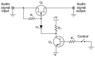
Question 30:
Explain the operation of this JFET audio signal switch circuit:
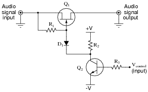
|
|
What sort of signal is necessary at pin Vcontrol to allow the audio signal to pass through the JFET, and what sort of signal turns the JFET off? Also, explain the purpose of each of these components in the audio switching circuit:
- �
- Diode D1
- �
- Resistor R1
- �
- Resistor R2
- �
- Resistor R3
Challenge question: what is the greatest peak audio signal voltage that this circuit will tolerate before misbehaving, in relation to the positive and negative DC supply voltages (+V and -V)?
Notes:
This circuit was taken from the February 2004 edition of Electronics World magazine, in an article written by Douglas Self. The article's original circuit showed component values, but I show it here in generic form, and somewhat rearranged.
Question 31:
If a junction field-effect transistor is subjected to several different gate-to-source voltages (Vgs), and the drain-to-source voltage (Vds) ßwept" through the full range for each of these gate voltage values, data for an entire "family" of characteristic curves may be obtained and graphed for the transistor:
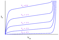
|
|
Identify the saturation, active, and breakdown regions on this graph.
What do these characteristic curves indicate about the gate voltage's control over drain current? How are the two signals related to each other?
The drain current regulation point is established by the gate voltage while in the äctive" region.
Notes:
Ask your students what the characteristic curves would look like for a perfect transistor: one that was a perfect regulator of drain current over the full range of drain-source voltage.
Question 32:
An important JFET parameter is VGS(off). Explain what this parameter means, and why it is important to us when selecting a JFET or designing a circuit around one.
Challenge question: is VGS(off) approximately the same for all models of JFET, or does it vary from transistor to transistor? Explain your answer.
Notes:
Ask your students what the "GS" subscript stands for in VGS.
Question 33:
What does the parameter IDSS mean for a JFET? How can we use this figure, along with VGS(off), and VGS, to calculate the amount of drain current (ID) for a JFET operating in its active region? Write the equation for the relationship between these four variables.
|
Follow-up question: how could you empirically determine the IDSS rating of a JFET? What sort of circuit would you have to set up in order to test and measure this transistor parameter?
Notes:
Be sure to ask students where they found this equation! It should be available from most basic electronics textbooks. Also, discuss the experimental circuit that would have to be constructed in order to test the shorted-gate drain current of a JFET. You might want to plan on having your students build this very circuit during class time as an exercise in using JFETs.
Question 34:
Calculate the amount of gate-to-source voltage necessary to regulate a JFET's drain current at a value of 2.5 mA, given the following transistor parameters:
- �
- VGS(off) = 3 volts
- �
- IDSS = 17 mA
Also, write the equation used for obtaining the value of VGS.
|
Notes:
Once students have found the standard drain current formula (transconductance equation), the rest is algebraic manipulation.
Question 35:
Cutoff voltage is not the same thing as pinch-off voltage, although the names seem quite similar. Give a concise definition for each of these field-effect transistor parameters, referencing them to a graph of characteristic curves if possible.
Follow-up question: which of these two parameters is more appropriate to consider when using an FET as a switch, and which is more appropriate when using an FET as a linear amplifier?
Notes:
This contrast and comparison is probably best shown on a graph of characteristic curves, but I leave this to the student to research!
Question 36:
The typical amount of current through a JFET gate terminal is far less than the typical amount of current through a BJT base terminal, for similar controlled currents (drain or collector, respectively). Explain what it is about the construction and/or use of the JFET that limits the input current to almost nothing during normal operation.
Notes:
If need be, refer back to a "cut-away" diagram of a JFET to help your students understand why the input impedance of a JFET is what it is.
Question 37:
The "transconductance" ratio (gm) of a field-effect transistor is a very important device parameter. In essence, it describes the amplifying power of the transistor. Give a mathematical definition for this parameter, and provide some typical values from transistor datasheets.
- �
- J110
- �
- J308
- �
- J309
- �
- J310
- �
- MPF 102
Challenge question: the "beta" ratio for a BJT (b) may be defined as the direct ratio of collector current to base current, or as the ratio between change in collector current and change in base current, as the following equations show.
|
|
By contrast, the transconductance of a FET is always defined in terms of change, and never in terms of a direct ratio:
|
|
Explain why this is.
Notes:
Ask your students to show you at least one datasheets for one of the listed transistors. With internet access, datasheets are extremely easy to locate. Your students will need to be able to locate component datasheets and application notes as part of their work responsibilities, so be sure they know how and where to access these valuable documents!
Discuss with your students why transconductance is measured in units of Siemens. Where else have they seen this unit of measurement? Why would it be an appropriate unit of measurement in this context?
Question 38:
Bipolar junction transistors are definitely unidirectional ("polarized") devices, able to handle electric currents in one particular direction through each terminal:
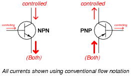
|
|
What about JFETs? Are they polarized just like BJTs? Explain your answer, complete with arrows showing proper directions of current through these two JFETs:
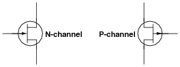
|
|
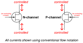
|
|
Follow-up question: explain why there is no "controlling" current (ideally) in a JFET.
Notes:
The fact that JFETs are bilateral devices rather than unilateral as bipolar junction transistors leads to some interesting applications whereby AC currents may be controlled! JFETs are often used in this capacity as AC signal switches, allowing a DC voltage to control passage or blocking of a low-amplitude AC signal such as an audio or RF signal prior to power amplification.
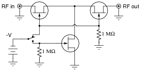
Question 39:
This is a switching circuit for video signals, or any other radio-frequency (RF), low-amplitude AC signals that one might need to switch on and off for a variety of different applications:
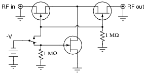
|
|
Identify the ön" and öff" states of the three JFETs in this circuit with the switch in the position shown in the schematic, and also determine whether the switch position shown in the diagram is for "passing" or "blocking" the RF signal from input to output.
|
|
With the switch in the position shown, the circuit will pass the RF signal from input to output.
Notes:
Ask your students to explain the problem-solving strategy(ies) they used to derive the correct answer for this question. How were they able to tell whether the transistors would be on or off? Ask them to explain the purpose of the 1 MW resistors. What might happen without them?
If time permits, discuss with your students the design of this circuit: why two "pass" transistors and one ßhunt" transistor? How critical is the magnitude of the -V switching control voltage?
The idea for this circuit came from a National Semiconductor application note on JFET circuits: Application Note 32, February 1970, page 13.
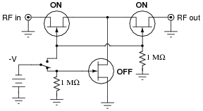
Question 40:
This is a switching circuit for video signals, or any other radio-frequency (RF), low-amplitude AC signals that one might need to switch on and off for a variety of different applications:
|
|
Identify the ön" and öff" states of the three JFETs in this circuit with the switch in the position shown in the schematic, and also determine whether the switch position shown in the diagram is for "passing" or "blocking" the RF signal from input to output.
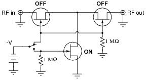
|
|
With the switch in the position shown, the circuit will block the RF signal from getting to the output.
Notes:
Ask your students to explain the problem-solving strategy(ies) they used to derive the correct answer for this question. How were they able to tell whether the transistors would be on or off? Ask them to explain the purpose of the 1 MW resistors. What might happen without them?
If time permits, discuss with your students the design of this circuit: why two "pass" transistors and one ßhunt" transistor? How critical is the magnitude of the -V switching control voltage?
The idea for this circuit came from a National Semiconductor application note on JFET circuits: Application Note 32, February 1970, page 13.
Question 41:
A very simple circuit that may be used as a current regulator in a DC circuit is this:
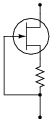
|
|
Draw a battery symbol and any necessary connecting wires to form a complete DC current source, that will attempt to supply a regulated amount of DC current through any given load.
|
|
Notes:
The direction of current through the JFET, when used as a current regulator in this fashion, is very important. Not so much for the JFET's sake, as for the sake of establishing the correct type of feedback (negative) to make the circuit self-regulating.
Discuss this circuit's operation with your students, asking them to determine the polarity of the resistor's voltage drop, and how that relates to the "pinching off" of the JFET.
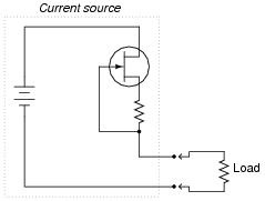
Question 42:
The following circuit is useful as a current regulator, the regulated current setpoint being established by the value of the resistor and the JFET's VGS(off) parameter:
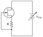
|
|
Despite wide variations in VDD, the current in this circuit will remain relatively constant. The reason this circuit works as it does is negative feedback. Explain what causes negative feedback to occur in this circuit, and why it has a stabilizing effect on the current.
Notes:
This is a simple example of negative feedback in action: one that does not require any AC analysis and all its associated considerations. Here it is just DC at work, and the students must determine what it is the JFET/resistor combination does in response to attempted changes in current that makes the current so stable.
Question 43:
Find one or two real junction field-effect transistors and bring them with you to class for discussion. Identify as much information as you can about your transistors prior to discussion:
- �
- Terminal identification (which terminal is gate, source, drain)
- �
- Continuous power rating
- �
- Typical transconductance
Notes:
The purpose of this question is to get students to kinesthetically interact with the subject matter. It may seem silly to have students engage in a ßhow and tell" exercise, but I have found that activities such as this greatly help some students. For those learners who are kinesthetic in nature, it is a great help to actually touch real components while they're learning about their function. Of course, this question also provides an excellent opportunity for them to practice interpreting component markings, use a multimeter, access datasheets, etc.