JFET amplifiers
Question 1:
| Don't just sit there! Build something!! |
Learning to mathematically analyze circuits requires much study and practice. Typically, students practice by working through lots of sample problems and checking their answers against those provided by the textbook or the instructor. While this is good, there is a much better way.
You will learn much more by actually building and analyzing real circuits, letting your test equipment provide the änswers" instead of a book or another person. For successful circuit-building exercises, follow these steps:
- 1.
- Carefully measure and record all component values prior to circuit construction, choosing resistor values high enough to make damage to any active components unlikely.
- 2.
- Draw the schematic diagram for the circuit to be analyzed.
- 3.
- Carefully build this circuit on a breadboard or other convenient medium.
- 4.
- Check the accuracy of the circuit's construction, following each wire to each connection point, and verifying these elements one-by-one on the diagram.
- 5.
- Mathematically analyze the circuit, solving for all voltage and current values.
- 6.
- Carefully measure all voltages and currents, to verify the accuracy of your analysis.
- 7.
- If there are any substantial errors (greater than a few percent), carefully check your circuit's construction against the diagram, then carefully re-calculate the values and re-measure.
When students are first learning about semiconductor devices, and are most likely to damage them by making improper connections in their circuits, I recommend they experiment with large, high-wattage components (1N4001 rectifying diodes, TO-220 or TO-3 case power transistors, etc.), and using dry-cell battery power sources rather than a benchtop power supply. This decreases the likelihood of component damage.
As usual, avoid very high and very low resistor values, to avoid measurement errors caused by meter "loading" (on the high end) and to avoid transistor burnout (on the low end). I recommend resistors between 1 kW and 100 kW.
One way you can save time and reduce the possibility of error is to begin with a very simple circuit and incrementally add components to increase its complexity after each analysis, rather than building a whole new circuit for each practice problem. Another time-saving technique is to re-use the same components in a variety of different circuit configurations. This way, you won't have to measure any component's value more than once.
Notes:
It has been my experience that students require much practice with circuit analysis to become proficient. To this end, instructors usually provide their students with lots of practice problems to work through, and provide answers for students to check their work against. While this approach makes students proficient in circuit theory, it fails to fully educate them.
Students don't just need mathematical practice. They also need real, hands-on practice building circuits and using test equipment. So, I suggest the following alternative approach: students should build their own "practice problems" with real components, and try to mathematically predict the various voltage and current values. This way, the mathematical theory "comes alive," and students gain practical proficiency they wouldn't gain merely by solving equations.
Another reason for following this method of practice is to teach students scientific method: the process of testing a hypothesis (in this case, mathematical predictions) by performing a real experiment. Students will also develop real troubleshooting skills as they occasionally make circuit construction errors.
Spend a few moments of time with your class to review some of the "rules" for building circuits before they begin. Discuss these issues with your students in the same Socratic manner you would normally discuss the worksheet questions, rather than simply telling them what they should and should not do. I never cease to be amazed at how poorly students grasp instructions when presented in a typical lecture (instructor monologue) format!
A note to those instructors who may complain about the "wasted" time required to have students build real circuits instead of just mathematically analyzing theoretical circuits:
What is the purpose of students taking your course?
If your students will be working with real circuits, then they should learn on real circuits whenever possible. If your goal is to educate theoretical physicists, then stick with abstract analysis, by all means! But most of us plan for our students to do something in the real world with the education we give them. The "wasted" time spent building real circuits will pay huge dividends when it comes time for them to apply their knowledge to practical problems.
Furthermore, having students build their own practice problems teaches them how to perform primary research, thus empowering them to continue their electrical/electronics education autonomously.
In most sciences, realistic experiments are much more difficult and expensive to set up than electrical circuits. Nuclear physics, biology, geology, and chemistry professors would just love to be able to have their students apply advanced mathematics to real experiments posing no safety hazard and costing less than a textbook. They can't, but you can. Exploit the convenience inherent to your science, and get those students of yours practicing their math on lots of real circuits!
Question 2:
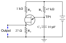
This relaxation oscillator circuit uses a resistor-capacitor combination (R1 - C1) to establish the time delay between output pulses:
|
|
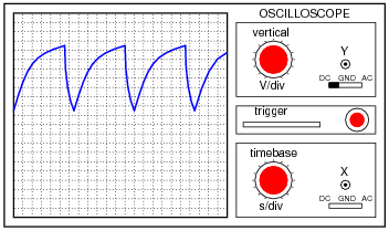
The voltage measured between TP1 and ground looks like this on the oscilloscope display:
|
|
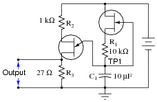
A slightly different version of this circuit adds a JFET to the capacitor's charge current path:
|
|
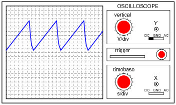
Now, the voltage at TP1 looks like this:
|
|
What function does the JFET perform in this circuit, based on your analysis of the new TP1 signal waveform? The straight-line charging voltage pattern shown on the second oscilloscope display indicates what the JFET is doing in this circuit.
Hint: you don't need to know anything about the function of the unijunction transistor (at the circuit's output) other than it acts as an on/off switch to periodically discharge the capacitor when the TP1 voltage reaches a certain threshold level.
Challenge question: write a formula predicting the slope of the ramping voltage waveform measured at TP1.
Answer to challenge question: Slope = [dv/dt] = [(ID)/C]
Notes:
Ask your students how they would know to relate "constant current" to the peculiar charging action of this capacitor. Ask them to explain this mathematically.
Then, ask them to explain exactly how the JFET works to regulate charging current.
Note: the schematic diagram for this circuit was derived from one found on page 958 of John Markus' Guidebook of Electronic Circuits, first edition. Apparently, the design originated from a Motorola publication on using unijunction transistors (Ünijunction Transistor Timers and Oscillators," AN-294, 1972).
Question 3:
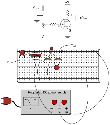
A student builds this transistor amplifier circuit on a solderless "breadboard":
|
|
The purpose of the potentiometer is to provide an adjustable DC bias voltage for the transistor, so it may be operated in Class-A mode. After some adjustment of this potentiometer, the student is able to obtain good amplification from the transistor (signal generators and oscilloscopes have been omitted from the illustration for simplicity).
Later, the student accidently adjusts the power supply voltage to a level beyond the JFET's rating, destroying the transistor. Re-setting the power supply voltage back where the student began the experiment and replacing the transistor, the student discovers that the biasing potentiometer must be re-adjusted to achieve good Class-A operation.
Intrigued by this discovery, the student decides to replace this transistor with a third (of the same part number, of course), just to see if the biasing potentiometer needs to be adjusted again for good Class-A operation. It does.
Explain why this is so. Why must the gate biasing potentiometer be re-adjusted every time the transistor is replaced, even if the replacement transistor(s) are of the exact same type?
Notes:
Ask your students to explain exactly what it is that causes the Q point of this amplifier circuit to change with each new transistor. Is it something in the transistor itself, or in some other part of the circuit?
Given the instability of gate biasing, should this method be used in mass-produced amplifier circuits? Ask your students to elaborate on why or why not.
Question 4:
The simple JFET amplifier circuit shown here (built with surface-mount components) employs a biasing technique known as self-biasing:
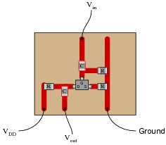
|
|
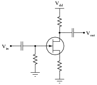
Self-biasing provides much greater Q-point stability than gate-biasing. Draw a schematic diagram of this circuit, and then explain how self-biasing works.
|
|
Self-biasing uses the negative feedback created by a source resistor to establish a "natural" Q-point for the amplifier circuit, rather than having to supply an external voltage as is done with gate biasing.
Notes:
The concept of negative feedback is extremely important in electronic circuits, but it is not easily grasped by all. Self-biasing of JFET transistors is a relatively easy-to-understand application of negative feedback, so be sure to take advantage of this opportunity to explore the concept with your students.
Ask your students to explain why Q-point stability is a desirable feature for mass-produced amplifier circuits, as well as circuits subject to component-level repair.
Question 5:
The voltage gain for a "bypassed" common-emitter BJT amplifier circuit is as follows:

|
|
Common-source JFET amplifier circuits are very similar:
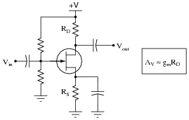
|
|
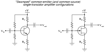
One of the problems with "bypassed" amplifier configurations such as the common-emitter and common-source is voltage gain variability. It is difficult to keep the voltage gain stable in either type of amplifier, due to changing factors within the transistors themselves which cannot be tightly controlled (r�e and gm, respectively). One solution to this dilemma is to ßwamp" those uncontrollable factors by not bypassing the emitter (or source) resistor. The result is greater AV stability at the expense of AV magnitude:
|
|
Write the voltage gain equations for both ßwamped" BJT and JFET amplifier configurations, and explain why they are similar to each other.
|
|
I'll let you explain why these two voltage gain approximations share the same form. Hint: it has something to do with the magnitudes of the currents through each transistor terminal!
Follow-up question: explain mathematically why the emitter/source resistances succeed in ßwamping" r�e and gm, respectively, in these more precise formulae. You should provide typical values for r�e and gm as part of your argument:
|
|
Notes:
Swamping is a common engineering practice, and one that students would do well to understand. It is unfortunate that parameters such as dynamic emitter resistance (r�e) and transconductance (gm) are so variable, but this does not have to be the end of the story. To be able to work around practical limitations such as these is the essence of engineering practice, in my opinion.
Question 6:
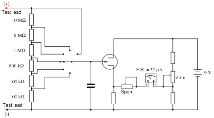
The circuit shown here is a precision DC voltmeter:
|
|
Explain why this circuit design requires the use of a field-effect transistor, and not a bipolar junction transistor (BJT).
Also, answer the following questions about the circuit:
- �
- Explain, step by step, how an increasing input voltage between the test probes causes the meter movement to deflect further.
- �
- If the most sensitive range of this voltmeter is 0.1 volts (full-scale), calculate the other range values, and label them on the schematic next to their respective switch positions.
- �
- What type of JFET configuration is this (common-gate, common-source, or common-drain)?
- �
- What purpose does the capacitor serve in this circuit?
- �
- What detrimental effect would result from installing a capacitor that was too large?
- �
- Estimate a reasonable value for the capacitor's capacitance.
- �
- Explain the functions of the "Zero" and "Span" calibration potentiometers.
- �
- 0.1 volts
- �
- 0.2 volts
- �
- 1.0 volts
- �
- 2.0 volts
- �
- 10 volts
- �
- 20 volts
The JFET is being used in the common drain configuration. A reasonable value for the capacitor would be 0.01 mF.
Notes:
This relatively simple DC voltage amplifier circuit provides a wealth of educational value, both for understanding the function of the JFET, and also for review on past electrical/electronics concepts.
Note: John Markus' Guidebook of Electronic Circuits, first edition, page 469, provided the inspiration for this circuit.
Question 7:
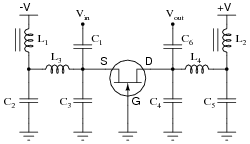
This is a schematic of an RF amplifier using a JFET as the active element:
|
|
What configuration of JFET amplifier is this (common drain, common gate, or common source)? Also, explain the purpose of the two iron-core inductors in this circuit. Hint: inductors L1 and L2 are often referred to as RF chokes.
Notes:
Be sure to ask your students why it would not be good for the RF signals to find their way to the DC power supply. There is more than one possible answer to this question!
This schematic was derived from an evaluation amplifier schematic shown in an ON Semiconductor J308/J309/J310 transistor datasheet.
Question 8:
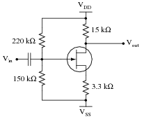
Calculate the approximate input impedance of this JFET amplifier circuit:
|
|
Explain why it is easier to calculate the Zin of a JFET circuit like this than it is to calculate the Zin of a similar bipolar transistor amplifier circuit. Also, explain how calculation of this amplifier's output impedance compares with that of a similar BJT amplifier circuit - same approach or different approach?
Notes:
Ask your students to explain why input impedance is an important factor in amplifier design. Why should we care how much input impedance an amplifier has?
Also, ask your students to explain why such high-value bias resistors (150 kW and 220 kW) would probably not be practical in a BJT amplifier circuit.
Question 9:
Define what a common-source transistor amplifier circuit is. What distinguishes this amplifier configuration from the other single-FET amplifier configurations, namely common-drain and common-gate? What configuration of BJT amplifier circuit does the common-source FET circuit most resemble in form and behavior?
Also, describe the typical voltage gains of this amplifier configuration, and whether it is inverting or noninverting.
The common-source amplifier configuration most resembles the common-emitter BJT amplifier configuration in both form and behavior.
Common-source amplifiers are characterized by moderate voltage gains, and an inverting phase relationship between input and output.
Notes:
The answers to the question may be easily found in any fundamental electronics text, but it is important to ensure students know why these characteristics are such. I always like to tell my students, "Memory will fail you, so you need to build an understanding of why things are, not just what things are."
One exercise you might have your students do is come up to the board in front of the room and draw an example of this circuit, then everyone may refer to the drawn image when discussing the circuit's characteristics.
Question 10:
Define what a common-gate transistor amplifier circuit is. What distinguishes this amplifier configuration from the other single-FET amplifier configurations, namely common-drain and common-source? What configuration of BJT amplifier circuit does the common-gate FET circuit most resemble in form and behavior?
Also, describe the typical voltage gains of this amplifier configuration, and whether it is inverting or noninverting.
The common-gate amplifier configuration most resembles the common-base BJT amplifier configuration in both form and behavior.
Common-gate amplifiers are characterized by moderate voltage gains, and a noninverting phase relationship between input and output.
Notes:
The answers to the question may be easily found in any fundamental electronics text, but it is important to ensure students know why these characteristics are such. I always like to tell my students, "Memory will fail you, so you need to build an understanding of why things are, not just what things are."
One exercise you might have your students do is come up to the board in front of the room and draw an example of this circuit, then everyone may refer to the drawn image when discussing the circuit's characteristics.
Question 11:
Define what a common-drain transistor amplifier circuit is. What distinguishes this amplifier configuration from the other single-FET amplifier configurations, namely common-source and common-gate? What configuration of BJT amplifier circuit does the common-drain FET circuit most resemble in form and behavior?
Also, describe the typical voltage gains of this amplifier configuration, and whether it is inverting or noninverting.
The common-drain amplifier configuration most resembles the common-collector BJT amplifier configuration in both form and behavior.
Common-drain amplifiers are characterized by low voltage gains (less than unity), and a noninverting phase relationship between input and output.
Notes:
The answers to the question may be easily found in any fundamental electronics text, but it is important to ensure students know why these characteristics are such. I always like to tell my students, "Memory will fail you, so you need to build an understanding of why things are, not just what things are."
One exercise you might have your students do is come up to the board in front of the room and draw an example of this circuit, then everyone may refer to the drawn image when discussing the circuit's characteristics.
Question 12:
Determine whether this amplifier circuit is inverting or noninverting (i.e. the phase shift between input and output waveforms):
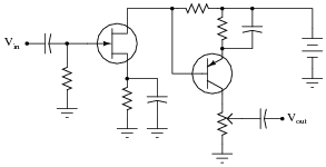
|
|
Be sure to explain, step by step, how you were able to determine the phase relationship between input and output in this circuit. Also identify the type of amplifier each transistor represents (common-???).
Notes:
There are several other questions you could ask about this amplifier circuit. For example:
- �
- How is the Q-point bias established for the JFET?
- �
- How is the Q-point bias established for the BJT?
- �
- What purpose does the potentiometer serve?
- �
- Is there another possible location for the potentiometer that would perform the same function?
Note: the schematic diagram for this circuit was derived from one found on page 36 of John Markus' Guidebook of Electronic Circuits, first edition. Apparently, the design originated from a Motorola publication on using field effect transistors ("Tips on using FET's," HMA-33, 1971).
Question 13:
It is a well-known fact that temperature affects the operating parameters of bipolar junction transistors. This is why grounded-emitter circuits (with no emitter feedback resistor) are not practical as stand-alone amplifier circuits.
Does temperature affect junction field-effect transistors in the same way, or to the same extent? Design an experiment to determine the answer to this question.
Notes:
The purpose of this question is to get students thinking in an experimental mode. It is very important that students learn to set up and run their own experiments, so they will be able to verify (or perhaps discover!) electronic principles after they have graduated from school. There will be times when the answers they seek are not to be found in a book, and they will have to "let the electrons teach them" what they need to know.
Remind your students that proper scientific experiments include both experimental and control subjects, so that results are based upon a comparison of measurements.
Question 14:
Identify what type of amplifier circuit this is, and also what would happen to the output voltage if Vin2 were to become more positive:
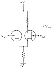
|
|
Notes:
Students should be able to relate this circuit to its bipolar transistor counterpart. Ask them to explain what advantages or disadvantages this circuit holds over a bipolar differential amplifier circuit.
Question 15:
The following circuit is a "multicoupler" for audio signals: one audio signal source (such as a microphone) is distributed to three different outputs:
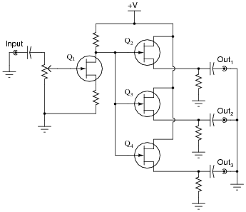
|
|
Suppose an audio signal is getting through from the input to outputs 2 and 3, but not through to output 1. Identify possible failures in the circuit that could cause this. Be as specific as you can, and identify how you would confirm each type of failure using a multimeter.
Notes:
Always be sure to spend plenty of time discussing troubleshooting scenarios with your students, because diagnostic skills are the highest level (and the most valuable) to develop.
Some of your students may be unfamiliar with the symbols used for the input and output jacks. Elaborate on this symbolism, if necessary.
Ask your students to identify the configuration (common-source, common-drain, or common-gate) of each JFET in this circuit, and how these respective configurations relate to the voltage gain (AV) of each amplification stage.
