Multi-stage transistor amplifiers
Question 1:
| Don't just sit there! Build something!! |
Learning to mathematically analyze circuits requires much study and practice. Typically, students practice by working through lots of sample problems and checking their answers against those provided by the textbook or the instructor. While this is good, there is a much better way.
You will learn much more by actually building and analyzing real circuits, letting your test equipment provide the änswers" instead of a book or another person. For successful circuit-building exercises, follow these steps:
- 1.
- Carefully measure and record all component values prior to circuit construction, choosing resistor values high enough to make damage to any active components unlikely.
- 2.
- Draw the schematic diagram for the circuit to be analyzed.
- 3.
- Carefully build this circuit on a breadboard or other convenient medium.
- 4.
- Check the accuracy of the circuit's construction, following each wire to each connection point, and verifying these elements one-by-one on the diagram.
- 5.
- Mathematically analyze the circuit, solving for all voltage and current values.
- 6.
- Carefully measure all voltages and currents, to verify the accuracy of your analysis.
- 7.
- If there are any substantial errors (greater than a few percent), carefully check your circuit's construction against the diagram, then carefully re-calculate the values and re-measure.
When students are first learning about semiconductor devices, and are most likely to damage them by making improper connections in their circuits, I recommend they experiment with large, high-wattage components (1N4001 rectifying diodes, TO-220 or TO-3 case power transistors, etc.), and using dry-cell battery power sources rather than a benchtop power supply. This decreases the likelihood of component damage.
As usual, avoid very high and very low resistor values, to avoid measurement errors caused by meter "loading" (on the high end) and to avoid transistor burnout (on the low end). I recommend resistors between 1 kW and 100 kW.
One way you can save time and reduce the possibility of error is to begin with a very simple circuit and incrementally add components to increase its complexity after each analysis, rather than building a whole new circuit for each practice problem. Another time-saving technique is to re-use the same components in a variety of different circuit configurations. This way, you won't have to measure any component's value more than once.
Notes:
It has been my experience that students require much practice with circuit analysis to become proficient. To this end, instructors usually provide their students with lots of practice problems to work through, and provide answers for students to check their work against. While this approach makes students proficient in circuit theory, it fails to fully educate them.
Students don't just need mathematical practice. They also need real, hands-on practice building circuits and using test equipment. So, I suggest the following alternative approach: students should build their own "practice problems" with real components, and try to mathematically predict the various voltage and current values. This way, the mathematical theory "comes alive," and students gain practical proficiency they wouldn't gain merely by solving equations.
Another reason for following this method of practice is to teach students scientific method: the process of testing a hypothesis (in this case, mathematical predictions) by performing a real experiment. Students will also develop real troubleshooting skills as they occasionally make circuit construction errors.
Spend a few moments of time with your class to review some of the "rules" for building circuits before they begin. Discuss these issues with your students in the same Socratic manner you would normally discuss the worksheet questions, rather than simply telling them what they should and should not do. I never cease to be amazed at how poorly students grasp instructions when presented in a typical lecture (instructor monologue) format!
A note to those instructors who may complain about the "wasted" time required to have students build real circuits instead of just mathematically analyzing theoretical circuits:
What is the purpose of students taking your course?
If your students will be working with real circuits, then they should learn on real circuits whenever possible. If your goal is to educate theoretical physicists, then stick with abstract analysis, by all means! But most of us plan for our students to do something in the real world with the education we give them. The "wasted" time spent building real circuits will pay huge dividends when it comes time for them to apply their knowledge to practical problems.
Furthermore, having students build their own practice problems teaches them how to perform primary research, thus empowering them to continue their electrical/electronics education autonomously.
In most sciences, realistic experiments are much more difficult and expensive to set up than electrical circuits. Nuclear physics, biology, geology, and chemistry professors would just love to be able to have their students apply advanced mathematics to real experiments posing no safety hazard and costing less than a textbook. They can't, but you can. Exploit the convenience inherent to your science, and get those students of yours practicing their math on lots of real circuits!
Question 2:
Why is it common for amplifier circuits to use multiple stages of transistors, rather than just one transistor (or two transistors in a push-pull circuit)? Describe some of the benefits of using multiple transistor stages.
Notes:
A fairly simple question, but useful to discuss nevertheless.
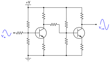
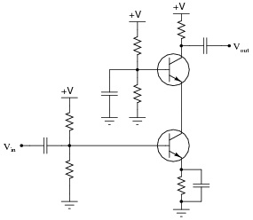
Question 3:
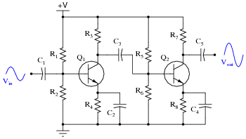
Describe the function of each component in this two-stage amplifier circuit:
|
|
Also, be prepared to explain what the effect of any one component's failure (either open or shorted) will have on the output signal.
- �
- R1 = Q1 biasing
- �
- R2 = Q1 biasing
- �
- R3 = Q1 load
- �
- R4 = Q1 stability (prevents thermal runaway)
- �
- R5 = Q2 biasing
- �
- R6 = Q2 biasing
- �
- R7 = Q2 load
- �
- R8 = Q2 stability (prevents thermal runaway)
- �
- C1 = Input signal coupling to Q1
- �
- C2 = AC bypass for Q1
- �
- C3 = Coupling between amplifier stages
- �
- C4 = AC bypass for Q2
- �
- C5 = Output signal coupling to load
- �
- Q1 = First-stage amplification
- �
- Q2 = Second-stage amplification
Notes:
The answers given in the Änswers" section are minimal: just enough to help students who may be struggling with the concepts. During discussion, I would expect more detail than these short phrases.
Be sure to challenge your students with hypothetical component failures in this circuit. Make sure they comprehend each component's function in this circuit, beyond memorizing a phrase!
Question 4:
In some applications where transistors must amplify very high currents, bipolar transistors are paralleled together so that their current ratings add:
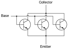
|
|
However, if transistors are directly paralleled as shown, reliability problems may develop. A better way of "ganging" multiple transistors together is to connect a low-value swamping resistor to each emitter terminal:

|
|
Explain what purpose these resistors serve in a paralleled transistor network. And what exactly does ßwamping" mean, anyway?
Follow-up question: can you think of any disadvantages to using swamping resistors in high-power circuitry?
Notes:
I once had the misfortune of performing component-level repair on a large power inverter (208 volt, three-phase) that used large "banks" of directly paralleled bipolar transistors for the final switching elements. These inverters had a bad habit of destroying transistors, and I noticed that invariably there would be only one or two transistors out of about a dozen on each heat sink rail that were blown - and I mean blown, holes blasted through the metal TO-3 cases! - while the rest were perfectly fine. These transistor banks did not employ swamping resistors, and so the current distribution between them was quite unbalanced.
In case students ask, you should let them know that swamping resistors are not just used in transistor banks. Large rectifier diode banks (where multiple diodes are paralleled) also benefit from swamping resistors.
As for applications where swamping resistors are impractical, it is possible to gain better reliability by using more transistors (or diodes) than necessary with an even current split. In other words, over-build the circuit.
Question 5:
In some applications where transistors must amplify very high currents, bipolar transistors are paralleled together so that their current ratings add. When this is done, it is a good idea to use swamping resistors at the transistor emitter connections to help ensure even balancing of currents:
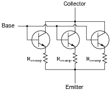
|
|
However, if we use MOSFETs instead of BJTs, we do not have to use swamping resistors:
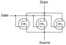
|
|
Explain why MOSFETs do not require swamping resistors to help evenly distribute current, while BJTs do.
Notes:
The answer given here is purposefully vague. Let your students do the necessary research! Tell them that manufacturers' application notes are valuable sources of information for questions such as this.
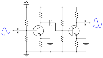
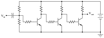
Question 6:
The first amplifier circuit shown here is direct-coupled, while the second is capacitively coupled.
|
|
|
|
Which of these two designs would be more suitable for use in a DC voltmeter circuit (amplifying a measured DC voltage)? What applications would the other amplifier design be suited for?
Follow-up question: in each of these amplifier circuits, identify the point at which the signal's phase becomes shifted by 180o. In other words, show where the voltage signal becomes inverted, and then inverted again, so that the output is in phase with the input.
Notes:
A good question to ask your students is, "What is bandwidth?" It is important that your students understand the basic concept of "bandwidth", and what factors influence it in a circuit.
Ask your students to suggest possible values (in microfarads) for the coupling capacitor in the second circuit, based on common resistor values (between 1 kW and 100 kW), and a modest audio frequency range (1 kHz to 20 kHz). No exact values are needed here, but it is important that they be able to make an approximate estimation of the necessary (minimum) capacitance, if for no other reason than to demonstrate their comprehension of the coupling capacitor's intended purpose.
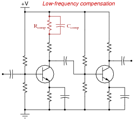
Question 7:
One of the problems with capacitively-coupled amplifier circuits is poor low-frequency response: as the input signal frequency decreases, all capacitive reactances increase, leading to a decreased voltage gain. One solution to this problem is the addition of a capacitor in the collector current path of the initial transistor stage:
|
|
Explain how the presence of this "compensating" capacitor helps to overcome the loss of gain normally experienced as a result of the other capacitors in the circuit.
Notes:
This technique is commonly used in video amplifier circuits, although a complete video amplifier circuit would not be this crude (no peaking coils).
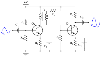
Question 8:
This two-stage transistor amplifier circuit is transformer-coupled:
|
|
What advantage(s) does a transformer-coupled amplifier have over circuits using other methods of coupling? Are there any disadvantages to using a transformer for signal coupling between transistor stages? Explain in detail.
Follow-up question: label the transformer's polarity using "dot" notation in order to achieve no inversion of signal from input to output (as shown).
Notes:
Ask your students to explain what impedance transformation is and why it is important, especially in amplifier circuits. This will be a good review of both transformer theory and the maximum power transfer theorem.
Regarding phase inversion, a fun challenge here is to have students specify the "dot convention" necessary for this particular transformer to obtain the non-inverting characteristic of this two-stage amplifier circuit. In other words, have them draw dots near the transformer windings (with the proper relative relationship) to produce the phasing shown by the sine-wave symbols in the diagram.
Question 9:
Suppose two engineers were debating where to place a potentiometer in this audio amplifier circuit, to be used as a volume control:
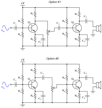
|
|
Which option would be better, and why? What ill effects could result from locating the potentiometer in the wrong place in this circuit?
Notes:
The purpose of this question is to make students realize that the biasing of each transistor stage is important in a multi-stage amplifier. One of the major challenges of designing a multi-stage amplifier is to ensure adequate signal coupling between stages without creating bias problems.
Question 10:
Radio-frequency amplifiers often use small inductors called peaking coils in the coupling circuitry between transistor stages. Describe the purpose of these inductors.
Notes:
The answer I gave for this question is very minimal, and is just enough to give your students a hint. Ask your students to explain why capacitive reactance is an issue in high-frequency transistor amplifier circuits, and why an inductor would be used to counter XC. Also, ask if there are any disadvantages to inserting peaking coils into amplifier circuits.
Question 11:
One design of push-pull audio amplifier uses two identical transistors and a center-tapped transformer to couple power to the load (usually a speaker, in an audio-frequency system):
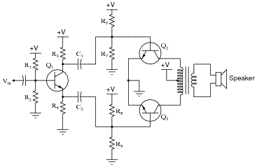
|
|
Unlike complementary-pair push-pull amplifier circuits, this circuit absolutely requires a preamplifier stage called a phase splitter, comprised here by transistor Q1 and resistors R3 and R4.
Explain what the purpose of the "phase splitter" circuit is, and why it is necessary to properly drive the power transistors Q2 and Q3.
Hint: determine the phase relationships of the voltage signals at the base, collector, and emitter terminals of transistor Q1, with respect to ground.
Follow-up question: typically, the collector and emitter resistors of the phase splitter circuit (R3 and R4 in this example) are equally sized. Explain why.
Notes:
Ask your students to qualitatively analyze the voltage signal waveforms at all parts of this circuit. When does Q1 conduct current? When does Q2 conduct current?
Also, discuss the operational class of this amplifier circuit. Is it Class B, or Class AB? What would need to be changed in order to shift the circuit's operational mode?
Explain to your students that this circuit topology was very common in the days of electron tube electronics, when there was no such thing as complementary active components (i.e., NPN versus PNP). Triode, tetrode, and pentode tubes are all positive-driven devices, conducting more current as the grid voltage becomes more positive. Thus, the only way to make a push-pull amplifier with electron tubes was to use a pair to drive the center-tapped winding of an audio power transformer, and use a phase splitter circuit to drive the two tubes.
Most modern (semiconductor) audio amplifier designs avoid the use of an audio output transformer. Ask your students why they think this may be the case.
Question 12:
Examine this push-pull audio amplifier circuit:
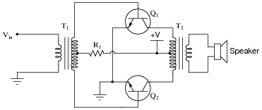
|
|
Answer the following questions about this circuit based on your analysis of it:
- �
- How is phase splitting accomplished in this circuit?
- �
- What is the purpose of resistor R1?
- �
- What would happen if resistor R1 failed open?
- �
- What would happen if the wire connecting the base of transistor Q2 to the input transformer (T1) were to fail open?
- �
- The input transformer T1 provides phase splitting.
- �
- R1 establishes the Q point of both transistors.
- �
- If R1 failed open, both transistors would go into cutoff mode.
- �
- If the wire connecting the base of transistor Q2 to the input transformer (T1) were to fail open, one-half of the output waveform would become clipped.
Notes:
Ask your students to give detailed reasons for their answers. The answers provided for this question are minimal - it is your job as the instructor to ensure students are thinking their way through this question, and not just repeating something they've read or heard from others.
Question 13:
The following amplifier circuit has a problem. Despite the presence of a strong input signal (as verified by an oscilloscope measurement at TP1), there is no sound coming from the speaker:
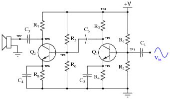
|
|
Explain a logical, step-by-step approach to identifying the source of the problem, by taking voltage signal measurements. Remember, the more efficient your troubleshooting technique is (the fewer measurements taken), the better!
Notes:
This question can easily occupy a large portion of your discussion time, so be sure to make room for it in your schedule!
A great way to help students grasp the concepts involved in this circuit as well as improve their troubleshooting technique, is to make a large-scale demonstration board of this circuit, which you can fault on the back side by disconnecting wires, opening or closing switches, etc. Then, have the students take an oscilloscope and practice finding problems in the circuit by voltage measurement only. I have built similar demonstration boards for my own classroom, and have found them to be extremely useful in building and assessing troubleshooting skills.
Question 14:
A common wideband transistor amplifier circuit is the cascode design, using common-emitter and common-base transistor stages:
|
|
What advantage(s) does the cascode amplifier have over "normal" single- or multi-stage amplifier designs? What, specifically, makes it well suited for high-frequency applications, such as RF (Radio Frequency) signal amplifiers?
Notes:
This is one of the few popular applications for the common-base transistor amplifier configuration, and it is a solution that has been implemented with field-effect transistors as well as bipolar transistors (and even electron tubes, before that!). Ask your students to explain how the circuit works, especially noting the voltage gain of each stage, and the locations of interjunction (Miller-effect) capacitances in the circuit.
Question 15:
Suppose the following three-stage transistor amplifier were constructed:
|
|
With no emitter swamping resistors anywhere in this circuit, the voltage gain of each stage is guaranteed to be large, but unstable as well. With three stages arranged like this, one feeding into the next, the final voltage gain will be very large, and very unstable.
However, if we add another resistor to the circuit (Rfeedback), something very interesting takes place. Suddenly, the amplifier circuit's overall voltage gain is decreased, but the stability of this gain becomes much improved:
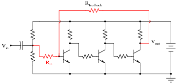
|
|
Interestingly, the voltage gain of such a circuit will be nearly equal to the quotient of the two highlighted resistors, Rfeedback and Rin:
|
This approximation holds true for large variations in individual transistor gain (b) as well as temperature and other factors which would normally wreak havoc in the circuit with no feedback resistor in place.
Describe what role the feedback resistor plays in this circuit, and explain how the addition of negative feedback is an overall benefit to this circuit's performance. Also, explain how you can tell this feedback is negative in nature ("degenerative").
We can tell that the feedback is negative in nature because it comes from an odd number of inverting amplifier stages (there is still an inverse relationship between output and input).
Follow-up question: how much effect do you suppose the replacement of a transistor with a slightly different b or r�e parameter would affect each circuit?
Notes:
Although the circuit shown is a little too crude to be practical, it does illustrate the power of negative feedback as a stabilizing influence.
The question regarding the de-generative nature of the feedback is an important one. Discuss with your students how one could not simply pick up the feedback signal from anywhere in the circuit!