TTL logic gates
Question 1:
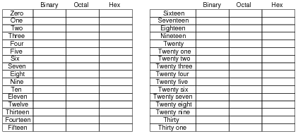
Counting practice: count from zero to thirty-one in binary, octal, and hexadecimal:
|
|
Notes:
In order to familiarize students with these ßtrange" numeration systems, I like to begin each day of digital circuit instruction with counting practice. Students need to be fluent in these numeration systems by the time they are finished studying digital circuits!
One suggestion I give to students to help them see patterns in the count sequences is "pad" the numbers with leading zeroes so that all numbers have the same number of characters. For example, instead of writing "10" for the binary number two, write "00010". This way, the patterns of character cycling (especially binary, where each successively higher-valued bit has half the frequency of the one before it) become more evident to see.
Question 2:
| Don't just sit there! Build something!! |
Learning to analyze digital circuits requires much study and practice. Typically, students practice by working through lots of sample problems and checking their answers against those provided by the textbook or the instructor. While this is good, there is a much better way.
You will learn much more by actually building and analyzing real circuits, letting your test equipment provide the änswers" instead of a book or another person. For successful circuit-building exercises, follow these steps:
- 1.
- Draw the schematic diagram for the digital circuit to be analyzed.
- 2.
- Carefully build this circuit on a breadboard or other convenient medium.
- 3.
- Check the accuracy of the circuit's construction, following each wire to each connection point, and verifying these elements one-by-one on the diagram.
- 4.
- Analyze the circuit, determining all output logic states for given input conditions.
- 5.
- Carefully measure those logic states, to verify the accuracy of your analysis.
- 6.
- If there are any errors, carefully check your circuit's construction against the diagram, then carefully re-analyze the circuit and re-measure.
Always be sure that the power supply voltage levels are within specification for the logic circuits you plan to use. If TTL, the power supply must be a 5-volt regulated supply, adjusted to a value as close to 5.0 volts DC as possible.
One way you can save time and reduce the possibility of error is to begin with a very simple circuit and incrementally add components to increase its complexity after each analysis, rather than building a whole new circuit for each practice problem. Another time-saving technique is to re-use the same components in a variety of different circuit configurations. This way, you won't have to measure any component's value more than once.
Notes:
It has been my experience that students require much practice with circuit analysis to become proficient. To this end, instructors usually provide their students with lots of practice problems to work through, and provide answers for students to check their work against. While this approach makes students proficient in circuit theory, it fails to fully educate them.
Students don't just need mathematical practice. They also need real, hands-on practice building circuits and using test equipment. So, I suggest the following alternative approach: students should build their own "practice problems" with real components, and try to predict the various logic states. This way, the digital theory "comes alive," and students gain practical proficiency they wouldn't gain merely by solving Boolean equations or simplifying Karnaugh maps.
Another reason for following this method of practice is to teach students scientific method: the process of testing a hypothesis (in this case, logic state predictions) by performing a real experiment. Students will also develop real troubleshooting skills as they occasionally make circuit construction errors.
Spend a few moments of time with your class to review some of the "rules" for building circuits before they begin. Discuss these issues with your students in the same Socratic manner you would normally discuss the worksheet questions, rather than simply telling them what they should and should not do. I never cease to be amazed at how poorly students grasp instructions when presented in a typical lecture (instructor monologue) format!
I highly recommend CMOS logic circuitry for at-home experiments, where students may not have access to a 5-volt regulated power supply. Modern CMOS circuitry is far more rugged with regard to static discharge than the first CMOS circuits, so fears of students harming these devices by not having a "proper" laboratory set up at home are largely unfounded.
A note to those instructors who may complain about the "wasted" time required to have students build real circuits instead of just mathematically analyzing theoretical circuits:
What is the purpose of students taking your course?
If your students will be working with real circuits, then they should learn on real circuits whenever possible. If your goal is to educate theoretical physicists, then stick with abstract analysis, by all means! But most of us plan for our students to do something in the real world with the education we give them. The "wasted" time spent building real circuits will pay huge dividends when it comes time for them to apply their knowledge to practical problems.
Furthermore, having students build their own practice problems teaches them how to perform primary research, thus empowering them to continue their electrical/electronics education autonomously.
In most sciences, realistic experiments are much more difficult and expensive to set up than electrical circuits. Nuclear physics, biology, geology, and chemistry professors would just love to be able to have their students apply advanced mathematics to real experiments posing no safety hazard and costing less than a textbook. They can't, but you can. Exploit the convenience inherent to your science, and get those students of yours practicing their math on lots of real circuits!
Question 3:
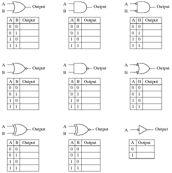
Identify each of these logic gates by name, and complete their respective truth tables:
|
|
|
|
Notes:
In order to familiarize students with the standard logic gate types, I like to given them practice with identification and truth tables each day. Students need to be able to recognize these logic gate types at a glance, or else they will have difficulty analyzing circuits that use them.
Question 4:
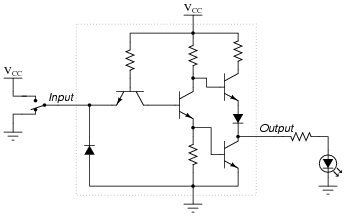
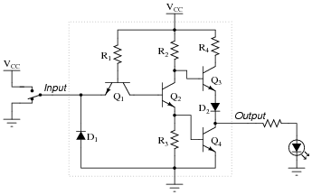
The simplest type of digital logic circuit is an inverter, also called an inverting buffer, or NOT gate. Here is a schematic diagram for an inverter gate constructed from bipolar transistors (transistor-to-transistor-logic, also known as TTL), shown connected to a SPDT switch and an LED:
|
|
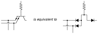
The left-most transistor in this schematic is actually not being used as a transistor, but rather it functions as a ßteering diode" network, like this:
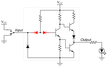
|
|
Determine the status of the LED in each of the input switch's two positions. Denote the logic level of switch and LED in the form of a truth table:

|
|

|
|
Notes:
Have your students explain the operation of this TTL circuit, describing how the inverse logic state is generated at the output terminal, from a given input state.
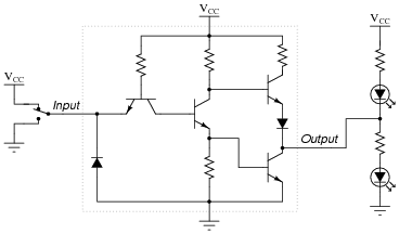
Question 5:
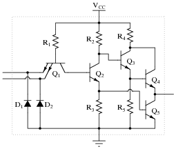
The following is an internal schematic of a TTL logic gate. Based on your analysis of the transistor circuit, determine what type of gate (AND, OR, NAND, NOR, XOR, etc.) it is:
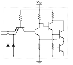
|
|
Hint: the double-emitter transistor is being used as a pair of diodes, and not as an amplifying device!
|
|
Notes:
TTL circuits are actually quite easy to analyze compared to analog amplifier circuits! Discuss with your students the use of a dual-emitter transistor as a ßteering" diode network: this is a trick used by IC manufacturers, to obtain three diodes for the "price" of one transistor.
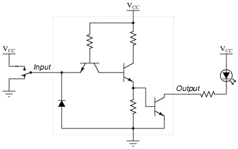
Question 6:
A very important concept to understand in digital circuitry is the difference between current sourcing and current sinking. For instance, examine this TTL inverter gate circuit, connected to a load:
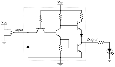
|
|
The output circuitry of this particular gate is commonly referred to as "totem-pole," because the two output transistors are stacked one above the other like figures on a totem pole. Is a gate circuit with a totem-pole output stage able to source load current, sink load current, or do both?
Follow-up question: does the input device driving this TTL gate circuit (the switch in this particular example) have to source current, sink current, or both?
Challenge question: explain how you would calculate the current sourcing and current sinking abilities of this logic gate circuit, if you were given the internal component values and parameters.
Notes:
The very important concept of sourcing versus sinking is best understood from the perspective of conventional current flow notation. The terms seem backward when electron flow notation is used to track current through the output transistor.
One point of confusion I've experienced among students is that current may go either direction (in or out) of a gate with totem-pole output transistors (able to sink or source current). Some students seem to have a conceptual difficulty with current going in to the output terminal of a gate circuit, because they mistakenly associate the öut" in output as being a reference to direction of current, rather than direction of information or data.
An analogy I've used to help students overcome this problem is that of two people carrying a long pole:
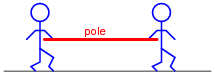
|
|
Suppose these people are in a dark, noisy room, and they use the pole as a means of simple communication between them. For example, one person could tug on the pole to get the other person's attention. Perhaps they could even develop a simple code system for communicating thoughts (1 tug = hello ; 2 tugs = good-bye ; 3 tugs = I think this is a silly way to communicate ; 4 tugs = let's leave this room ; etc.). If one of the persons pushes on the pole rather than pulls on the pole to get the other person's attention, does the direction of the pole's motion change the direction of the communication between the two persons? Of course not. Well, then, does the direction of current through the output terminal of a gate change the direction that information flows between two interconnected gates? Whether a gate sources current or sinks current to a load has no bearing on the öutput" designation of that gate terminal. Either way, the gate is still "telling the load what to do" by exercising control over the load current.
Question 7:
A very important concept to understand in digital circuitry is the difference between current sourcing and current sinking. For instance, examine this open-collector TTL inverter gate circuit, connected to a load:
|
|
Open-collector gates are specially designated in their schematic symbols by a marker within the gate shape:

|
|
Is this gate circuit able to source load current, sink load current, or do both?
Follow-up question #1: what would need to be added to the gate circuit shown, in order for it to have the ability to source load current as well as sink load current?
Follow-up question #2: explain how you would calculate current sinking ability of this logic gate circuit, if you were given the internal component values and parameters.
Notes:
The very important concept of sourcing versus sinking is best understood from the perspective of conventional current flow notation. The terms seem backward when electron flow notation is used to track current through the output transistor.
One point of confusion I've experienced among students is that current may go either direction (in or out) of a gate with totem-pole output transistors (able to sink or source current). Some students seem to have a conceptual difficulty with current going in to the output terminal of a gate circuit, because they mistakenly associate the öut" in output as being a reference to direction of current, rather than direction of information or data.
An analogy I've used to help students overcome this problem is that of two people carrying a long pole:

|
|
Suppose these people are in a dark, noisy room, and they use the pole as a means of simple communication between them. For example, one person could tug on the pole to get the other person's attention. Perhaps they could even develop a simple code system for communicating thoughts (1 tug = hello ; 2 tugs = good-bye ; 3 tugs = I think this is a silly way to communicate ; 4 tugs = let's leave this room ; etc.). If one of the persons pushes on the pole rather than pulls on the pole to get the other person's attention, does the direction of the pole's motion change the direction of the communication between the two persons? Of course not. Well, then, does the direction of current through the output terminal of a gate change the direction that information flows between two interconnected gates? Whether a gate sources current or sinks current to a load has no bearing on the öutput" designation of that gate terminal. Either way, the gate is still "telling the load what to do" by exercising control over the load current.
Ask your students to explain what the term öpen-collector" means with reference to a TTL logic gate. How does this type of gate compare with normal ("totem pole" output) TTL gates?
Question 8:
Based on an analysis of a typical TTL logic gate circuit (consult a datasheet for a TTL logic gate if you need an internal schematic diagram for a gate circuit), determine what logic state is ässumed" by a TTL gate input when left "floating" (disconnected).
What ramification does this have for us when choosing input devices for TTL logic gates? If, for instance, we wished to use a single-pole, single-throw (SPST) switch as the input device for a TTL logic gate, what is the best way to connect such a device to a TTL input? Should the switch connect the TTL input to VCC when closed, or should it connect the input to VEE when closed? Why does it matter? Explain your answer in detail.
Notes:
For review, ask your students what the symbols VCC and VEE mean with reference to TTL circuits.
Proper TTL ëtiquette" is vitally important for students to understand, if they are to successfully build digital circuits (especially when interfacing TTL with other types of logic!).
Question 9:
A logic probe is a very useful tool for working with digital logic circuits. It indicates "high" and "low" logic states by means of LED's, giving visual indication only if the voltage levels are appropriate for each state.
Here is a schematic diagram for a logic probe built using comparators. Each comparator has a threshold adjustment potentiometer, so that it may be set to indicate its respective logic state only if the signal voltage is well within the range stated by the logic manufacturer:
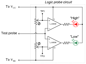
|
|
When this logic probe circuit is connected to the VCC and VEE power supply terminals of a powered TTL circuit, what voltage levels should test points TP1 and TP2 be adjusted to, in order for the probe to properly indicate "high" and "low" TTL logic states? Consult a datasheet for the quad NAND gate numbered either 74LS00 or 54LS00. Both are legacy TTL integrated circuits.
Follow-up question: given the standard VCC voltage level of 5.0 volts for TTL circuits, and assuming the use of LEDs that drop 1.7 volts at 20 mA, calculate an appropriate resistance value for the two LED current-limiting resistors.
Challenge question: the logic probe circuit shown is minimal in component count. To make a more practical and reliable probe, one would probably want to have reverse-polarity protection (in case someone were to accidently connect the probe backward across the power supply) as well as decoupling for immunity against electrical noise. Add whatever necessary components you think there should be in this circuit to provide these features.
Notes:
The most obvious lesson of this question is to introduce (or review as the case may be) the purpose and operation of a logic probe. However, this question is also a veiled introduction (or review) of TTL logic levels.
Question 10:
A student builds the following digital circuit on a solderless breadboard (a "proto-board"):
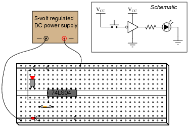
|
|
The DIP circuit is a TTL hex inverter (it contains six ïnverter" or "NOT" logic gates), but only one of these gates is being used in this circuit. The student's intent was to build a logic circuit that energized the LED when the pushbutton switch was unactuated, and de-energized the LED when the switch was pressed: so that the LED indicated the reverse state of the switch itself. However, in reality the LED fails to energize no matter what state the switch is in.
First question: how would you use a multimeter as a logic probe to check the logic states of points in this circuit, in order to troubleshoot it?
Second question: suppose you checked the logic states of pin #1 on the IC, for both states of the switch (pressed and unpressed), and found that pin #1 was always "high". How does this measurement indicate the student's design flaw in this circuit? How would you recommend this design flaw be corrected?
The problem with this student's circuit is the input switch: it does not provide a solid "low" state when open. Rather, the inverter's input is left "floating" when the switch is unactuated. There is more than one way to fix this design flaw, but I'll leave the details up to you!
Notes:
Discuss the problem of "floating" or "high-Z" states with your students. It is always a good idea to eliminate ambiguous logic states such as this in the circuits you build.
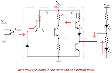
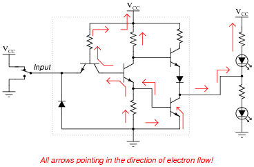
Question 11:
Draw the paths of all currents in this circuit with the input in a "low" state:

|
|
Now, draw the paths of all currents in this circuit with the input in a "high" state:
|
|
Where is the power supplied for each LED? What relationship is there between the load current (LED) and the gate input current (through the SPDT switch)?
Also, explain how you would calculate the values for appropriate LED current-limiting resistors in this circuit.
|
|
|
|
In each scenario, the LED's power is supplied by VCC and ground: the DC power source. Note that the input switch merely "tells" the output what to do rather than handle actual load current, just like the inputs of an operational amplifier or comparator.
Notes:
The utility of conventional flow notation (as opposed to electron flow) becomes especially apparent in this answer, as the upper circuit is the one sourcing current and the lower circuit is the one sinking current.
As with operational amplifiers, I find it necessary to point out to some students that the inputs of a logic gate circuit do not sink or source load current. This fact underscores the need to supply DC power to the logic gate for proper operation.
Question 12:
The digital circuit shown here is a unanimous-yea vote detector. Votes are cast by eight different voters by the setting of switches in either the closed (yea) or open (nay) positions. According to the logic function provided by the TTL gates, the LED will energize if and only if all switches are closed:
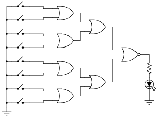
|
|
As is common in digital circuit schematics, the power supply (VCC) is omitted for the sake of simplicity. This is analogous to the omission of power supply connections in many operational amplifier circuit schematics.
If we were to draw a truth table for this circuit, how large (number of rows and columns) would the table have to be?
Suppose we wished to modify this circuit, such that an electromechanical bell would ring whenever a unanimous-yea vote was cast, rather than merely lighting a small LED. The bell we have in mind to use is rather large, its solenoid coil drawing 3 amps of current at a voltage of 12 volts DC: well beyond the final gate's ability to source. How could we modify this circuit so that the final gate is able to energize this bell instead of just an LED?
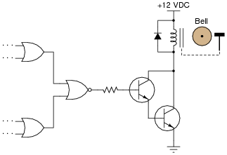
|
|
Follow-up question: explain why pullup resistors are not required in this circuit.
Challenge question: sometimes engineers and technicians alike overlook the most elegant (beautifully simple) solutions in their quest to solve a problem. The solution shown here, while practical, solves the problem by adding components to the circuit. Can you think of a way we might build a unanimous-yea vote detector using fewer components than the original LED circuit?
Notes:
Ask your students why we might want to use a Darlington pair instead of a single transistor for the final output "driver" circuit. Also, ask them why we need to have a resistor connected between the gate output and the transistor base. Why not just directly connect the gate's output to the base of the transistor?
You might want to challenge your students with this question: "Suppose the person who built this circuit used open-collector gates throughout. As a whole, it would not function, neither for lighting the LED nor for ringing the bell. However, only one of the gates would need to have the standard `totem-pole' output in order for the circuit to function properly. Which gate is it?"
Question 13:
Totem-pole TTL gates usually differ greatly in their maximum source current versus maximum sink current (IOH versus IOL). Identify which current rating is usually greater, and also explain why this is.
Notes:
It should be noted that totem-pole TTL gates can actually source far more current than what is advertised without sustaining damage. The severe limitation on sourcing current is more a function of staying within the permitted output voltage margins for TTL than it is a function of chip heating. Thus, you may generally use a totem-pole TTL gate to source 20 mA to an LED without harm, though the "high" state output voltage (when the LED is lit) will be significantly below the acceptable threshold for a TTL gate input.
Question 14:
In high-speed digital circuits, a very important logic gate parameter is propagation delay: the delay time between a change-of-state on a gate's input and the corresponding change-of-state on that gate's output. Consult a manufacturer's datasheet for any TTL logic gate and report the typical propagation delay times published there.
Also, explain what causes propagation delay in logic gates. Why isn't the change in output state instantaneous when an input changes states?
Follow-up questions: What difference is there between high-to-low output transitions versus low-to-high output transitions for the gate you researched? Which transition is faster?
Notes:
I purposely omitted answers for this question, not only because I want students to do the research on their own, but also because it makes it more interesting when students consult different datasheets and derive different answers (for different logic "families")!
Question 15:
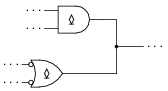
Logic gates are limited in the number of gate inputs which one output can reliably drive. This limit is referred to as fan-out:
|
|
Explain why this limit exists. What is it about the construction of TTL logic gates that inherently limits the number of TTL inputs that any one TTL output can drive? What might happen if this limit is exceeded?
Locate a datasheet for a TTL gate and research its fan-out limit. Note: this number will vary with the particular type of TTL referenced (L, LS, H, AS, ALS, etc.).
Notes:
For the relatively simple digital circuits that beginning students build, fan-out is rarely a problem. More likely is that students will try to drive a load that is too "heavy," causing the same voltage level problem.
Question 16:
Explain why it is generally a very bad design practice to connect the outputs of different logic gates together, like this:
|
|
However, there are certain specific circumstances in which "paralleling" gate outputs is acceptable. For instance, it is okay to parallel two or more inverters, like this:
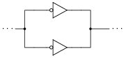
|
|
No damage will be done if open-collector gate outputs are paralleled, either (although the resulting logic function may be strange):
|
|
And finally, gates that have tri-state outputs may also have their outputs paralleled if certain precautions are taken:
|
|
What, specifically, causes gates to be damaged by "paralleling" their outputs? Generally speaking, what principle must be followed in order to "parallel" logic gate outputs without risk of damage? Explain how each of the three acceptable "paralleled" scenarios shown here meet this criterion.
Suggestion: the issue of multiple gates having to output logic voltage signals onto common conductors ("busses") is called bus contention. Try looking for this term in your research to see what useful information you find on paralleled gates!
Notes:
The given answer cuts to the heart of the matter, but I want students to elaborate on the details. Specifically, why each of the three acceptable paralleled circuits avoids risk of damage. Make sure you spend adequate time discussing "tri-state" outputs as well. Ask your students to explain what the three output states of a "tri-state" gate are.
Question 17:
An important parameter of logic gate circuitry is noise margin. What exactly is "noise margin," and how is it defined for logic gates?
Specifically, how much noise margin do digital circuits exclusively composed of TTL gates have?
Note: you will need to consult TTL gate datasheets to answer this question properly.
Notes:
This question, to be answered properly, involves more than just a definition of "noise margin." Students must first discover that there is a difference between voltage compliance levels for gate inputs versus outputs, then recognize that the difference constitutes a "margin" that imposed AC voltage ("noise") must not exceed. They must then present their answer in terms of manufacturer specifications, obtained in datasheets. In summary, there is a lot of research that must occur to answer this question, but the results will be worth it!
Question 18:
Predict how the operation of this logic gate circuit will be affected as a result of the following faults. Consider each fault independently (i.e. one at a time, no multiple faults):
|
|
- �
- Diode D1 fails open:
- �
- Diode D1 fails shorted:
- �
- Diode D2 fails open:
- �
- Resistor R1 fails open:
- �
- Resistor R2 fails open:
- �
- Resistor R4 fails open:
For each of these conditions, explain why the resulting effects will occur.
- �
- Diode D1 fails open: No effect.
- �
- Diode D1 fails shorted: Output always in high state, possible damage to circuit when input switch is in high state.
- �
- Diode D2 fails open: Gate can sink current in low output state, but cannot source current in high output state.
- �
- Resistor R1 fails open: Output always in high state.
- �
- Resistor R2 fails open: Gate can sink some current in low output state, but cannot source current in high output state. Gate may have trouble attaining a solid "low" output state as well.
- �
- Resistor R4 fails open: Limited ability to source current in high output state.
Notes:
The purpose of this question is to approach the domain of circuit troubleshooting from a perspective of knowing what the fault is, rather than only knowing what the symptoms are. Although this is not necessarily a realistic perspective, it helps students build the foundational knowledge necessary to diagnose a faulted circuit from empirical data. Questions such as this should be followed (eventually) by other questions asking students to identify likely faults based on measurements.
Question 19:
Predict how the operation of this logic gate circuit will be affected as a result of the following faults. Consider each fault independently (i.e. one at a time, no multiple faults):
|
|
- �
- Diode D1 fails open:
- �
- Diode D1 fails shorted:
- �
- Diode D2 fails open:
- �
- Resistor R1 fails open:
- �
- Resistor R2 fails open:
- �
- Transistor Q2 emitter terminal fails open:
- �
- Transistor Q3 emitter terminal fails open:
For each of these conditions, explain why the resulting effects will occur.
- �
- Diode D1 fails open: No effect.
- �
- Diode D1 fails shorted: Output always in high state, possible damage to circuit when input switch is in high state.
- �
- Diode D2 fails open: No effect.
- �
- Resistor R1 fails open: Output always in high state.
- �
- Resistor R2 fails open: Gate can sink some current in low output state, but cannot source current in high output state. Gate may have trouble attaining a solid "low" output state as well.
- �
- Transistor Q2 emitter terminal fails open: Output always in high state.
- �
- Transistor Q3 emitter terminal fails open: Gate can sink current in low output state, but cannot source current in high output state.
Notes:
The purpose of this question is to approach the domain of circuit troubleshooting from a perspective of knowing what the fault is, rather than only knowing what the symptoms are. Although this is not necessarily a realistic perspective, it helps students build the foundational knowledge necessary to diagnose a faulted circuit from empirical data. Questions such as this should be followed (eventually) by other questions asking students to identify likely faults based on measurements.
Question 20:
In TTL circuitry, one side of the DC power supply is usually labeled as "VCC", while the other side is labeled as "VEE". Why is this? What do the subscripts "CC" and ËE" represent?
VEE = Power supplied to emitter side of bipolar transistors.
Follow-up question: Since TTL circuits use NPN transistors exclusively, what polarities must each of these labels represent?
Notes:
This question is a good review of bipolar junction transistor theory.
Question 21:
True story: once upon a time, there was a machine shop containing a number of computer-controlled machine tools (lathes, mills, grinders, etc.), where one of the machines proved to be very "finicky" when starting. Sometimes, it would function properly when you pushed the "Start" button, and other times it refused to work at all. The problem was so bad, it got to the point where the machinists responsible for operating this tool became almost superstitious about it, performing a ritual dance before pressing the "Start" button, whimsically hoping to improve their luck.
An electrician was called to service this machine, but he could find nothing wrong with the electrical power circuitry. All of the high-voltage equipment (transformers, relays, motors, motor control circuits, etc.) seemed to be in good working order. The problem, whatever it was, resided within the machine's electronic control computer. The computer was not sending the ßtart" signal to the motor control circuits when the "Start" button was pushed.
An electronics technician was called to troubleshoot the computer, and he was able to fix it in a matter of minutes. The problem, he said, was the computer's DC power supply: the voltage regulator was out of adjustment. With just a twist of a potentiometer, the technician was able to "trim" the regulated voltage to 5.00 volts, right where it should be for TTL circuitry.
The power supply voltage was not very far from 5.00 volts before the technician adjusted it. How far is the supply voltage allowed to deviate for TTL logic circuits, and still have guaranteed proper operation? Consult one or more IC datasheets for legacy TTL logic circuits (not the newer high-speed CMOS 54HCxx and 74HCxx chips) to obtain your answer.
Notes:
This true story was told to me by one of my former students, who had some previous experience with electronics maintenance prior to enrolling in my class. The moral of this story, of course, is the sensitivity of TTL logic circuits to power supply voltage variations. This will (and should!) surprise many of your students, who are probably used to seeing the rather wide voltage limits of opamps and other analog circuitry.
Question 22:
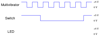
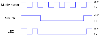
In this circuit, an AND gate is used to give a toggle switch control over the blinking of an LED:
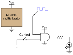
|
|
The ästable multivibrator" is nothing more than an oscillator that produces a square-wave signal at a low frequency, at standard TTL voltage levels (0 and +5 volts).
Plot the output waveform for the gate (i.e. the voltage signal to the LED), given the following input conditions:
|
|
Hint: it helps in your analysis of digital waveforms if you first write a truth table for the gate under consideration, for your reference.
|
|
Notes:
Many students find the waveform analysis of digital circuits intimidating at first, until they understand that it is nothing more than a graphical representation of "0" and "1" logic states over time. Ask your students to share their "tips" on how to relate waveforms to truth tables, and in particular how they answered this particular question.
Just for fun, you might want to ask your students to identify where in time the toggle switch is open, and where it is closed. Some students may answer backwards to this question, if they haven't carefully considered how the toggle switch is connected in this circuit!
Question 23:
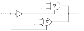
What does it mean if you see a logic gate symbol in a schematic diagram with a strange-looking "S" figure drawn inside of it?

|
|
Notes:
Schmitt trigger gates are indispensable for certain logic circuit applications. It is important that students recognize their function and utility.
Incidentally, this question provides a good opportunity to review magnetic hysteresis curves, since it's probably been awhile since students last studied electromagnetism theory!
Question 24:
For a true TTL gate (not high-speed CMOS), what is the default logic state of an input line that is left floating (neither connected to VCC nor Ground)? Explain why this is.
Notes:
The given answer does not provide enough detail to explain why TTL inputs tend to float high, so I recommend you display an internal TTL gate schematic for your students to analyze and comment on in class.
Question 25:
Explain why the allowable power supply voltage range for a true TTL (not high-speed CMOS) logic gate is so narrow. What is the typical range of supply voltages for a true TTL gate, and why can't this type of logic gate operate from a wider range of voltages as CMOS gates can?
Notes:
Many of the old 74xx and 74LSxx logic circuits are considered obsolete, but may still be found in a lot of operating equipment! It is not uncommon to have students mistakenly research the datasheets of a newer logic family such as 74HCxx which has different power supply requirements than traditional TTL. Be prepared to elaborate on the difference(s) between these IC families if and when your students encounter this confusion!