Solid State Relays are available almost everywhere these days, however they remain very expensive. Therefore, your efforts to build one yourself pays off. Especially since it only needs a handful components and the circuitry is simple and straightforward.
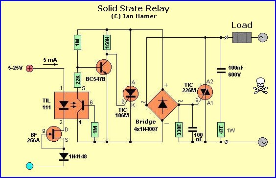
A Solid State Relay is actually not a relay at all. There is no 'relay' present, just the electronics which does the switching. It works the same way as a relay; you can use a low voltage to switch a higher voltage or better. This 'relay' is positioned in between one of the 115/220V AC wires although it is common practice to leave the neutral wire the way it is and switch the phase or hot wire. See diagram for 'LOAD'.
As long as thereis no dc voltage present (left side of circuit diagram), the phototransistor within the TIL111 blocks and so no current is present. To make sure of that the base of the TIL111 is fed to the emitter (e) via an 1M resistor. This method prevents the base of transistor BC547B going low and thus remains biased 'on'. The collector is thus also low, and consequently the gate (g) of the TIC106M thyristor, which remains in the 'off' state. Through the 4-diode bridge rectifier circuit there is no current, except for the miniscule basis and collector current of the BC547B which is not enough over the 330 ohm resistor to switch on the TIC226M Triac. The current through the 'Load' is thus very very small.
With a certain input voltage, say 5 volt, the diode inside the TIL111 lights up and activates the phototransistor. The voltage drop over the 1Meg ohm resistor in series with the 22K resistor increases to a certain set point that it will block the BC547B transistor. The collector current at that moment will follow that of the AC voltage to a certain value which will activate the Thyristor. This creates a sufficient large voltage drop over the 330 ohm resistor to switch the Triac 'on'. The voltage over the Triac at that moment is only a couple volts so that the practically the whole 115/220 AC voltage is over the 'Load'.
The Triac is protected via the 100nF capacitor and the 47 ohm resistor, the 100nF
capacitor over the 330 ohm resistor is to prevent unwanted biasing of the Triac created by small spikes. To create the
posibility to switch this circuit with different voltages, a FET BF256A has been added. This FET acts like a
current-source by means of connecting the source (s) with the gate (g). What this means is that this FET determines the
current through the TIL111, no matter what voltage is put on the input (within certain tolerances ofcourse). The diode
1N4148 is to protect the circuit in case of polarity reversal.
(Tony: The TIL111 is a so called 'optoisolator' with an NPN output and can be replaced with a NTE3042)
A good point of a circuit like this is the seperation of the DC and AC voltages, so
this circuit could be used in a variety of applications, up to approximately 1.5 KiloWatt, if you mount the Triac on a
large cooling-rib.
The 'M' indicator noted on the Triac means it is a 600volt type, a 'D' stands for 400volt. So make sure you go for the
M type.
(Tony: The NTE replacements for this circuit are 600volt types which is more than sufficient for our 110/115VAC.)
Also, if you decide to make a pcb for this circuit, to create sufficient space between the AC lines and
don't make these AC tracks too narrow.
Published & Translated from Dutch into English with
permission of Jan Hamer, The Netherlands.