Unlike the ideal op-amp (Fig. 5-1),
the op-amp that is used in more realistic circuits today,
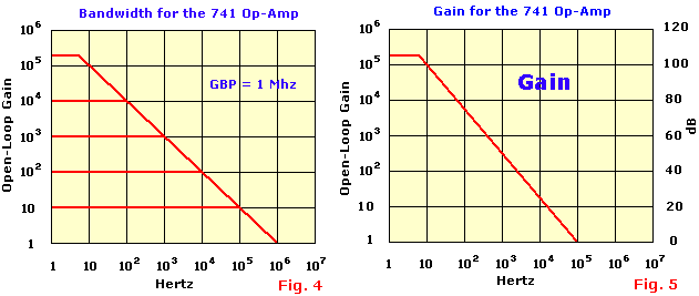
does not have infinite gain and bandwidth. Look at Open-loop gain in Fig. 4 above, it is graphed for a type 741
op-amp as a function of frequency. At very low frequencies, the open-loop gain of an op-amp is constant, but starts
to taper off at about 6Hz or so at a rate of -6dB/octave or -20dB/decade (an octave is a doubling in frequency,
and a decade is a ten-fold increase in frequency). This decrease continues until the gain is unity, or 0 dB.
The frequency at which the gain is unity is called the unity gain frequency or fT.
Maybe the first factor in the consideration of a specific op-amp is its "gain-bandwidth product" or GBP.
For the response curve of Fig. 4, the product of the open-loop gain and frequency is a constant at any point on
the curve, so that: GBP = AolBW
Graphically, the bandwidth is the point at which the closed-loop gain curve intersects the open-loop curve, as shown
in Fig. 5 for a family of closed-loop gains. For a more practical design situation, the actual design of an op-amp
circuit should be approximately 1/10 to 1/20 of the open-loop gain at a given frequency. This ensures that the
op-amp will function properly without distortion. As an example, using the response in Fig. 4, the closed-loop gain
at 10Khz should be about 5 to 10, since the open-loop gain is 100 (40dB).
One additional parameter is worth mentioning, the Transient Response, or rise time is the time that it
takes for the output signal to go from 10% to 90% of its final value when a step-function pulse is used as an input
signal, and is specified under close-loop conditions. From electronic circuit theory, the rise time is related to the
bandwidth of the op-amp by the relation: BW = 0.35 / rise time
Open-Loop Gain:
Lets have a look how the 'ideal' amplifier would look like in Fig. 5-1. The search for an ideal amplifier is, of course, a futile
exercise. The characteristics of the operational amplifier are good enough, however, to allow us to treat it as
ideal. Below are some amplifier properties that make this so. (Please realize that these ratings are next
to impossible to achieve).
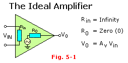
     1. Gain--infinite
     2. Input impedance--infinite
     3. Output impedance--zero
     4. Bandwidth--infinite
     5. Voltage out--zero (when voltages into
           each other are equal)
     6. Current entering the amp at either
           terminal--extremely small
The "operation" referred to mathematical operations, such as addition, integration, etc. An exact equivalent of the
ideal Op-Amp is called a "nullor" and it is composed of new elements -- the nullator and the norator. The
input to the op-amp is the nullator (i.e. no voltage or current), while the output is the norator (i.e. any voltage or
current). These two components give the device its ideal characteristics.
Power Supply:
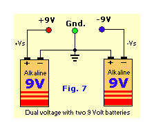
In general op-amps are designed to be powered from a dual or bipolar voltage supply which is typically in the range of
+5V to +15Vdc with respect to ground, and another supply voltage of -5V to -15Vdc with respect to ground, as
shown in Fig. 7. Although in certain cases an op-amp, like the LM3900 and called a 'Norton Op-Amp', may be powered
from a single supply voltage.
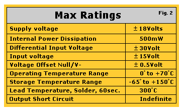
Electrical Ratings:
Electrical characteristics for op-amps are usually specified for a certain (given) supply voltage and ambient
temperature. Also, other factors may play an important role such as certain load and/or source resistance.
In general, all parameters have a typical minimum/maximum value in most cases.
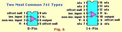 Fig. 6 - The two
most common types are shown in the diagram on the right. Depending on the application, the 8-pin version is used
the most, worldwide. Actually, there is a third type in the form of a metal-can but is obsolete and, by my knowledge,
no longer used. I have two of these metal-can types and keep them as a 'gone-by' memory.
Fig. 6 - The two
most common types are shown in the diagram on the right. Depending on the application, the 8-pin version is used
the most, worldwide. Actually, there is a third type in the form of a metal-can but is obsolete and, by my knowledge,
no longer used. I have two of these metal-can types and keep them as a 'gone-by' memory.
Definition of 741-pin functions: (Refer to the internal 741 schematic of Fig. 3)
Pin 1 (Offset Null): Offset nulling, see Fig. 11. Since the
op-amp is the differential type, input offset voltage must be controlled so as to minimize offset. Offset voltage is
nulled by application of a voltage of opposite polarity to the offset. An offset null-adjustment potentiometer may be
used to compensate for offset voltage. The null-offset potentiometer also compensates for irregularities in the
operational amplifier manufacturing process which may cause an offset. Consequently, the null potentiometer is
recommended for critical applications. See 'Offset Null Adjustment' for method.
Pin 2 (Inverted Input): All input signals at this pin will be inverted
at output pin 6. Pins 2 and 3 are very important (obviously) to get the correct input signals or the op amp can not do its work.
Pin 3 (Non-Inverted Input): All input signals at this pin will be
processed normally without inversion. The rest is the same as pin 2.
Pin 4 (-V): The V- pin (also referred to as Vss) is the
negative supply voltage terminal. Supply-voltage operating range for the 741 is -4.5 volts (minimum) to -18 volts
(max), and it is specified for operation between -5 and -15 Vdc. The device will operate essentially the
same over this range of voltages without change in timing period. Sensitivity of time interval to supply voltage
change is low, typically 0.1% per volt. (Note: Do not confuse the -V with ground).
Pin 5 (Offset Null): See pin 1, and Fig. 11.
Pin 6 (Output): Output signal's polarity will be the opposite
of the input's when this signal is applied to the op-amp's inverting input. For example, a sine-wave at the inverting
input will output a square-wave in the case of an inverting comparator circuit.
Pin 7 (posV): The V+ pin (also referred to as Vcc) is the
positive supply voltage terminal of the 741 Op-Amp IC. Supply-voltage operating range for the 741 is +4.5 volts
(minimum) to +18 volts (maximum), and it is specified for operation between +5 and +15 Vdc. The device will
operate essentially the same over this range of voltages without change in timing period. Actually, the most
significant operational difference is the output drive capability, which increases for both current and voltage range
as the supply voltage is increased. Sensitivity of time interval to supply voltage change is low, typically 0.1% per
volt.
Pin 8 (N/C): The 'N/C' stands for 'Not Connected'. There is
no other explanation. There is nothing connected to this pin, it is just there to make it a standard 8-pin package.
 Experiments:
You are given the opportunity to play with and analyze experiments to demonstrate the principles, concepts, and
applications of a couple of these basic configured op-amps.
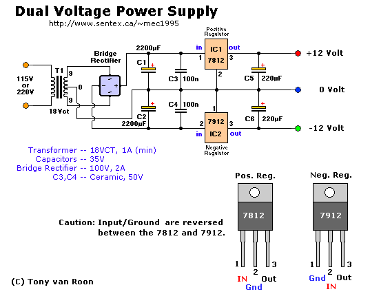
If you have already a dual-voltage power supply (positive/negative), that would make things allot easier for you.
If not, build this Dual Volt Powersupply listed at the bottom of the page to get you started.
This power supply has two non-adjustable voltages; +12Vdc and -12Vdc. However, in general, a very simple and cheap
power supply can be rigged up with two 9 Volt alkaline batteries and does the job in most, if not all, cases. Personally I like to
approach a project more professionally and build the dual 12 volt powersupply. Nice project 'in-between' while learning op-amps.
Bread Board Modules:
A bread board module, or just 'breadboard',
is a board manufactured of plastic with a couple 100 tiny holes with tiny sockets in them connected electrically
together and in the center of the breadboard a grove to hold a plastic panel for leds, pots and switches.
They measure about 6 by 2 inches and come in white, gray and blue. The blue kind is called 'BimBoard' and made in the UK.
I purchased mine back in 1980 from ElectroSonic in Toronto Canada and its
still working fine. The gray and white models are manufactured in the U.S. and Canada. They all work. Radio Shack
and the European Tandy are both selling their own version and they work fine too.
The Bread Board Design System is also available, if you can afford it, and would be preferred if you intend to do a
lot more experimenting in the future. This system contains everything you need already build-in, like the
powersupply, jacks, switches, leds, function generator and lots more goodies. Kindah nice to have everything in one
place.
The Norton Op-Amp:
 It is not my intention to confuse you with a different type of op-amp so I will
just mention a couple points about this op-amp.
It is not my intention to confuse you with a different type of op-amp so I will
just mention a couple points about this op-amp.
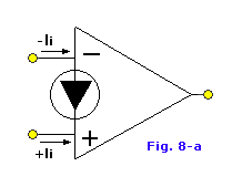
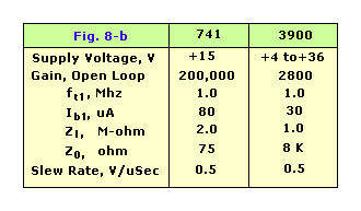
The Norton op-amp, or current-differencing amplifier, is designed to operate from a single ended supply. Wow, that is
truly fantastic. You can use a voltage anywhere from +4V to a whopping +36V!
The Norton op-amp referred to here is the LM3900 and is the best known type made by National Semiconductor.
This chip contains four op-amps in a single 14-pin package. The picture in Fig. 8-a shows the symbol for the Norton
op-amp. As you may notice it is somewhat different than the normal op-amp symbol. Fig. 8-b shows the major
parameters of relevance between the LM741 and the LM3900 op-amps.
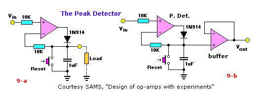 The Peak Detector
The peak detector is a circuit that "remembers" the peak value of a signal. As shown in Fig. 9-a, when a
positive voltage is fed to the noninverting input after the capacitor has been momentarily shorted (reset),
the output voltage of the op-amp forward biases the diode and charges up the capacitor. This charging last until the
inverting and noninverting inputs are at the same voltage, which is equal to the input voltage. When the noninverting
input voltage exceeds the voltage at the inverting input, which is also the voltage across the capacitor, the capacitor
will charge up to the new peak value. Consequently, the capacitor voltage will always be equal to the greatest
positive voltage applied to the noninverting input.
Once charged, the time that the peak detector "remembers" this peak value is typically several minutes and depends
on the impedance of the load that is connected to the circuit. Consequently, the capacitor will slowly discharge
towards zero. To minimize this rate of discharge, a voltage follower can be used to buffer the detector's output
from any external load, as shown in Fig. 9-b. Momentarily shorting the capacitor to ground
will immediately set the output to zero.
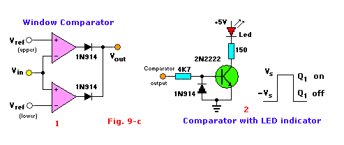 The Comparator
A 'comparator' is circuit that
compares an input voltage with a reference voltage. The output of the comparator then indicates whether the input
signal is either above or below the reference voltage. As shown for the basic circuit in Fig. 9-c(1)
, the output voltage approaches the positive supply voltage when the input signal is slightly greater than the
reference voltage, Vref. When the input is slightly less than the reference, the op-amp's output approaches the
negative supply voltage. Consequently, the exact threshold is dominated by the op-amp's input offset voltage, which
should be nulled out. Fig. 9-c(2) shows a Led indicator which input is connected to the
output Vout of the comparator.
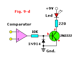
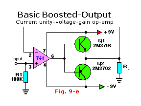
Fig. 9-d(left) The output polarity of the op-amp switches from positive to negative, it is
inconvenient to keep reversing the voltmeter leads to keep polarity correct. One way to overcome that problem is to
use an indicator light to tell the output state. The circuit show on the left uses a transistor to switch a led on
or off depending on the comparator's output state. When the op-amp output is 8.5 volts, the transistor switches on
the led via the 220 ohm current-limiting resistor. When the output is -8.5 volts the transistor is cut-off turning
off the led. Transistor choice is not critical; it can be any common type NPN device. Any type of silicon diode will
protect the transistor. Fig. 9-e(right). The output on pin 6 switches (repeatedly) from
positive to negative and so either bias Q1 (NPN) or Q2 (PNP and activates RL
which is the resistive load. Just a basic circuit to show you what exactly a 'Boosted-Output' circuit does.
 The Instrumentation Amplifier
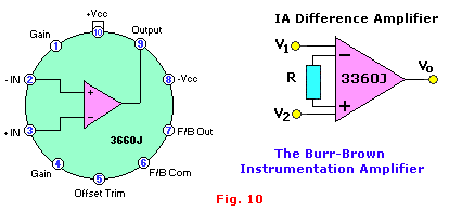
There are many types of op-amps who are designed for a specific purpose like the Instrumentation Amplifier from
Burr-Brown.(see Fig. 10) In this example we are talking about the 3660J type. It can be used in both balanced and
unbalanced systems, like a Wheatstone Bridge circuit. This does not mean in any way that the instrumentation amp
cannot be used for other applications, on the contrary, it is in many a case preferred because of the unique
parameters of this device.
Keep this in mind as a rule-of-thumb:
An operational amplifier circuit will not work at all unless:
1. External feedback limits the gain or desired response to a design value.
2. Both inputs have direct-current return path to ground of a similar reference.
3. The input frequencies and required gain are well within the performance limitations of
the op-amp used.
Offset Null Adjustment Procedure for the uA741:
Offset null adjustments differ with the application (e.i. Inverting or Non-Inverting Amplifier). Offset-null
potentiometers are not placed on design schematics as they would detract from a design. For practice, perform
the following Offset Null adjustment if you wish:
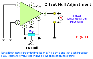 1. Adjust the 10K pot(entio)meter to its center position.
2. Connect the potmeter outside leads between pins 1 and 5 of the op-amp.
Make sure that the power is applied to the design application.
3. Connect the wiper of the potmeter to the negative supply voltage.
4. Ensure that input signals are zero or null and that pins 2 and 3 have a
dc return to ground.
5. Measure the output with a dc meter and obtain zero null by adjusting the
potentiometer.
This is just one method and recommended nulling procedure for the uA741 type op-amp. Always look for,
and follow the particular procedure as specified by that chip manufacturer. Procedures may become obsolete or updated
and changed when improved op-amp versions come on the market.
 Burr-Brown:
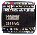
Look at this beauty at the right. It is a 20-pin 3656AG Isolation Amplifier made by Burr-Brown (valued at $487.00US in 2007).
Just wanted to show the chip because of its uniqueness. This gem measures about 22 x 28mm and is part of my personal
collection. The engineers of Burr-Brown have surely done a marvelous job more than once.
Planning Your Prototype or Experiment:
Planning the layout of your experiments could be important, especially with large circuits. Use this [lay-out sheet]
to plan your components layout on the bread board, if you wish. Remove every component and all wires from previous experiments.
Important: Before starting to insert components into the breadboard, make sure
all power and signal connections are removed and the power source disconnected. And if required, take the glue/dirt
of the components' legs before inserting them into the sockets, it is very hard if not impossible to get it cleaned
out.
A couple circuit examples:
Below are a couple circuit examples you can play and experiment with to understand the working of a 741 op-amp hands
on. If you are serious about electronics I strongly recommend buying a book or two about Op-Amps for your
experimenting pleasures.
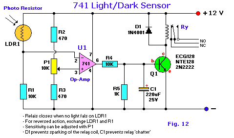
Fig. 12 - Light Sensor
This is a really nice circuit to play with. When there is NO light falling on the sensor, the relay closes.
When light falls on the LDR, the relay opens. To reverse the situation just exchange LDR and R1. Example uses for
this circuit: Dark-room, Automatic door-lock, closet, Shed Alarm, etc.
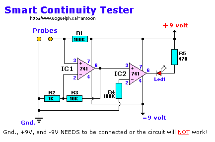
Fig. 13 - Smart Continuity Tester
Occasionally you need a continuity test between two points in an electronic circuit. Unfortunately, most continuity
testers are prone to "lie". They don't do that deliberately, but if they see a small resistance, they still
tell you that you have continuity. They just don't know any better. This unit is different. If you have continuity
it will tell you so. And if you're reading even a low resistance through a component, the unit will tell you that
as well. The unit uses two 741 op-amps. It offers a short-circuit test current of less than 200uA. It detects
resistance values of less than 10 ohms. Nicest of all, it will not break down a PN junction. The device has come in
handy in my own shop for debugging electronic circuits. Nowadays I use the 'Latching' Continuity Tester.
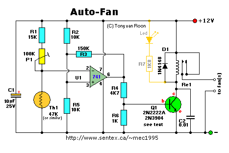
Fig. of Auto-Fan Circuit
A fun little circuit using a 741 op-amp and a NTC (Negative Temperature Coefficient) to cycle between two set
temperatures and switch a fan on and off.
Click here for the complete project: [Auto-Fan]
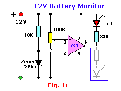
Fig. 14 - 12V Battery Monitor
The 100 Kilo-ohm trimmer pot controls the set point of this circuit to a 'high' point like 12.5 or something, so
adjust it to the point you wish the LED to light up. To monitor a 'low' point, and have the led light up when the
battery has drained to a certain point, connect the led (via the 330 ohm resistor) to ground (in the blue-boxed area).
The led is the high-brightness or ultra-bright type for maximum visibility. The trimpot in the schematic is a 10-turn
type for better accuracy, but basically any type will do.
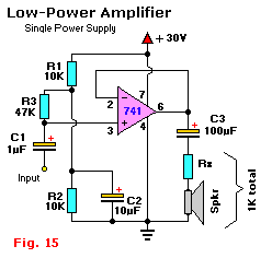
Fig. 15 - Low Power Amplifier
This is a simple low power amplifier with a single powersupply. The Rx resistor + the resistance of the speaker should
equal 1000 ohm. Example: speaker is 150 ohm. Rx is 1000 - 150 = 850 ohm. Closest available value is 860 ohm. I know what
your thinking; what about the 30 volt? Isn't the max 15 volt? Yes, but positive and negative they combine 30 volt.

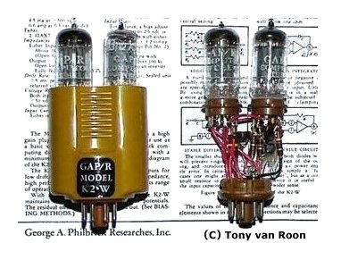 At the left you see a picture of a K2-W tubes general purpose
computing Op-Amp from George A. Philbrick Researches. This type was first introduced in 1952, more than a decade before
the first transistorized version. The op-amp is shown with and without its bakelite shell. What a beauty!
The first solid-state monolithic op-amp, designed by Bob Widlar, offered to the public in 1963 was the uA702 manufactured by
Fairchild Semiconductors but it had very weird supply voltages such as +12 and -6 volts and had a tendency to burn
out when it was temporarily shorted. Despite all these little shortcomings this device was the best in its day. It
contained just nine transistors and sold for about $300.00 US which limited the sales to the Military and Aerospace
consumers.
At the left you see a picture of a K2-W tubes general purpose
computing Op-Amp from George A. Philbrick Researches. This type was first introduced in 1952, more than a decade before
the first transistorized version. The op-amp is shown with and without its bakelite shell. What a beauty!
The first solid-state monolithic op-amp, designed by Bob Widlar, offered to the public in 1963 was the uA702 manufactured by
Fairchild Semiconductors but it had very weird supply voltages such as +12 and -6 volts and had a tendency to burn
out when it was temporarily shorted. Despite all these little shortcomings this device was the best in its day. It
contained just nine transistors and sold for about $300.00 US which limited the sales to the Military and Aerospace
consumers.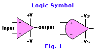
 Supply Voltage (+/-Vs):
The maximum voltage (positive and negative) that can be safely used to feed the op-amp.
Supply Voltage (+/-Vs):
The maximum voltage (positive and negative) that can be safely used to feed the op-amp.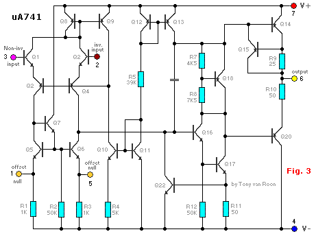
![[lay-out sheet]](bblayout.gif)