Vc = total supply voltage to circuit
THE LOOP FILTER:
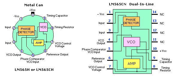
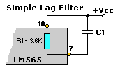
In almost all applications, it will be desirable to filter the signal at the output of the phase detector (Pin 7).
A simple lag filter may be used for wide closed loop bandwidth applications such as modulation following where the
frequency deviation of the carrier is fairly high (greater than 10%), or where wide-band modulation signals must be
followed.
For narrow band applications where narrow noise bandwidth is desired, such as applications involving tracking a
slowly varying carrier, a lead lag filter should be used. In general the damping factor for the loop becomes quite
small resulting in large overshoot and possible instability in the transient response of the loop.
Abbreviations:
AFC   -  Automatic Frequency Control
AM    -  Amplitude Modulation
CCO   -  Current Controlled Oscillator
CO    -  Controlled Oscillator
COS   -  Carrier Operating System
DTL   -  Diode-Transistor-Logic
FC    -  Frequency Control
FM    -  Frequency Modulation
FSK   -  Frequency Shift Keying
IC    -  Integrated Circuit
OS    -  Operating System
PLL   -  Phase-Lock Loop
SCA   -  Subsidiary Communications Authorization (Hidden Radio)
TTL   -  Transistor-Transistor-Logic
VCO   -  Voltage Controlled Oscillator
VCV   -  VCO Correction Voltage
AM - Amplitude Modulation
CCO - Current Controlled Oscillator
CO - Controlled Oscillator
COS - Carrier Operating System
DTL - Diode-Transistor-Logic
FC - Frequency Control
FM - Frequency Modulation
FSK - Frequency Shift Keying
IC - Integrated Circuit
OS - Operating System
PLL - Phase-Lock Loop
SCA - Subsidiary Communications Authorization (Hidden Radio)
TTL - Transistor-Transistor-Logic
VCO - Voltage Controlled Oscillator
VCV - VCO Correction Voltage
To see an example of a working PLL doing its job, check out the circuit below of Fig. 8.
This schematic diagram shows a so-called SCA adapter. The abbreviation "SCA" stands for
Subsidiary Communications
Authorization. It is used for 'hidden' messages, music, etc. on a normal hidden section of the FM band.
It is based on a 67-KHz subcarrier that is placed on a station's main FM carrier. It is even possible to have multiple
subcarriers, some carrying digital data, audio, data encryption, coded messages, and more. Subcarrier transmissions
have no effect on standard FM mono and stereo bands and are fully compatible with all existing radios. This circuit
can be hooked up to most FM tuners with a minimum of fuss. Low in cost, it uses just a few readily available IC's.
The use of a Printed Circuit Board for this design is recommended.
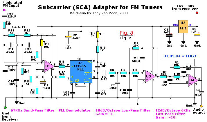
Parts List for the SCA Adapter

Semiconductors:                             C18 = 560pF, Polystyrene
U1,U3,U4 = TL071, FET OpAmp                 C19 = 220pF, Ceramic disc
      U2 = LM565, Phase-Locked-Loop
      U5 = LM7812, 12V Regulator            Resistors:
                                           (All resistors are 1/4W, 5% precision
Capacitors:                                 units unless otherwise noted.)
     C1 = 4.7uF/16V, electrolytic             R1 = 20K, 2% precision
     C2 = 2.2uF/16V, electrolytic             R2 = 18K
     C3 = 1uF/16V, electrolytic		   R3-R8 = 10K
     C4 = 1uF/35V, electrolytic		  R9,R10 = 1K8
  C5,C6 = .22uF, metalized Polyester     R11-R14 = 1100 ohm, 2% precision
     C7 = .033uF, metalized Polyester        R15 = 1K
     C8 = .022uF, metalized Polyester    R16,R17 = 560
     C9 = .0068uF, metalized Polyester       R18 = 10K, miniature vertical
    C10 = .0056uF, metalized Polyester                  trim-pot
C11-C14 = .0022uF, metalized Polyester       R19 = 5K, miniature vertical
C15-C17 = .001uF, metalized Polyester                  trim-pot
A Versatile PLL:
One of the most versatile PLL systems, seen particularly in Citizen Band receivers, is the UNIDEN 858.
The figure below shows a block diagram of the system. Let's work through it step by step and see what we can
discover.
The reference crystal in this case is 10.24 MHz, but note that in this instance the reference crystal is not
oscillating at the reference frequency--its signal is passed through a 1024 divider to give us a reference
frequency of 10 KHz. This 10 KHz reference signal is passed to the phase detector.
Now we know that the signal coming from the VCO must be divided to 10 KHz before being applied to the phase
detector--but notice one thing: in this system our VCO must oscillate at around 36 MHz to give us the correct
output frequency. This frequency is going to take a lot of dividing to get it down to the 10 KHz reference
frequency.
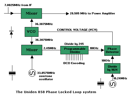 So here a cunning method has been used to convert the VCO frequency to a workable value before division. This
is where the 11.2858 MHz crystal comes into play. It's an overtone oscillator producing an output on the third
overtone of the crystal's fundamental frequency--ie 33.8575 MHz. This signal is then mixed with the VCO output,
the difference frequency being around 2 to 3 MHz. This signal can then be divided to 10 KHz quite simply and
applied to the phase detector.
So here a cunning method has been used to convert the VCO frequency to a workable value before division. This
is where the 11.2858 MHz crystal comes into play. It's an overtone oscillator producing an output on the third
overtone of the crystal's fundamental frequency--ie 33.8575 MHz. This signal is then mixed with the VCO output,
the difference frequency being around 2 to 3 MHz. This signal can then be divided to 10 KHz quite simply and
applied to the phase detector.
Before we get too involved in some actual circuit frequencies, let's look more closely at the frequency divider.
We see that it is a programmable divider, it can be set to divide by any amount from 1 to 399. The input data
to the divider is binary coded decimal (BCD) and is applied to pins 13 through 22 on the actual integrated circuit.
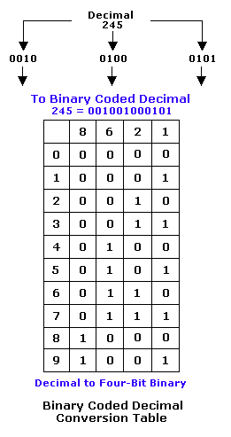 What is BCD? It's a method of expressing a decimal value as a four-bit binary number. The units in the decimal
number are expressed as a four-bit binary number, as are the tens, then the hundreds, etc. For example, decimal
251 would require three four-bit conversions: 1 is expressed as 0001; 5 becomes 0101; and 2 equals 0010. The final
figure is the chain of the three four-bit numbers: 251 equals 0010 0101 0001 in BCD.
What is BCD? It's a method of expressing a decimal value as a four-bit binary number. The units in the decimal
number are expressed as a four-bit binary number, as are the tens, then the hundreds, etc. For example, decimal
251 would require three four-bit conversions: 1 is expressed as 0001; 5 becomes 0101; and 2 equals 0010. The final
figure is the chain of the three four-bit numbers: 251 equals 0010 0101 0001 in BCD.
The divider has 10 inputs. These inputs can be set with a BCD code in the range 0 to 399 which equates to 400
channels. For channel 399 the four-bit BCD code would be 0011-1001-1001 (3-9-9).
So there are a total of 400 possible input combinations to the programmable divider, which theoretically means 400
operating frequencies, provided the radio frequency stages of the transceiver remain in tune or are tuned accordingly.
A logic (1) is represented by a +5V input level and a logic (0) by zero volts. If the input to the divider is
supplied with the BCD code for 146 (0001 0100 0110) then the input signal will appear at the output divided by 146.
Another point worth mentioning is that the VCO signal is not the final transmit frequency. All necessary processing
of the signal to be transmitted is performed before the PLL sage is reached. The output of the VCO is then mixed with
the intermediate frequency (IF) and the difference frequency produced is the actual transmit frequency.
Conversely, during receive operation, the VCO and the incoming signal are heterodyned to produce the IF frequency.
A Worked Example:
Let's take the desired output of 28.505 MHz, the VCO will be 7.8025 MHz higher (the IF frequency). The VCO therefore is
46.3075 MHz. THis is fed to the mixer along with a 33.8575 MHz signal derived from the third overtone of the 11.2858 MHz
crystal oscillator.
The 36.3075 MHz and 33.8675 MHz signals mix to produce a difference frequency of 2.45 MHz. Now the divider must be set
to divide the 2.45 MHz frequency down to 10 KHz. This requires a BCD code on the data inputs equivalent to 245 decimal
(divide-by 245). The logic levels applied to the BCD inputs would be 10 0100 0101.
The 10 KHz signal produced by the divider is phase detected with the stable 10 KHz reference frequency from the crystal
oscillator and a control voltage applied back to the VCO. After a very brief period the circuit will establish a lock.
Changing the divide-by number will change the output frequency in 10 KHz steps over a maximum frequency range of
400 x 10 KHz = 4 MHz. Incrementing or decrementing the divider will alter the VCO frequency by 10 KHz. So the channel
spacing in this case is 10 KHz.
If you think there is some relationship between the 10 KHz reference frequency and the 10 KHz channel steps, the you're
right! If 5 KHz channel spacing was required, all that would be necessary is to change the 1024 divider to a 2048 divider.
The 858 chip has provision on board for this -- pin 7 can be toggled between high and low to change from 1024 to 2048.
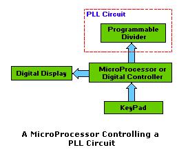
A microprocessor can be added to the PLL circuit to control the logic fed to the programmable divider. Such systems are
common in modern communications receivers/transmitters (see diagram below). Now a whole new scope of functionality is
available. The microprocessor, also named µP, can be told what to do from a keypad--and its internal program can
do things like change frequency, memorize frequencies, scan a range of frequencies, or operate between different programmable
transmit and receive frequencies, and much more. The microprocessor can even re-tune the VCO and other parts of the
transceiver to give extremely broadband coverage. An alternative to re-tuning the VCO is to have several VCO's and have the
microprocessor switch the appropriate one into circuit for the desired frequency range.
You now should have a very good idea of the way PLL frequency synthesis systems work. More complex systems do exist but they
are merely extensions of what has been described. Some modern communications equipment may use not one, but several PLL's,
and even PLL's within PLL's.
Copyright and Credits:
Some quotations are from the book: "The Art of Electronics", by Horowitz and Hill, listed below.
SCA Adapter copyright by Hands-On Electronics(Jan. 1989) and Gernsback Publishing (No longer in business).
Ron Bertrand VK2DQ, some quotations from his article "The Basics of PLL Frequency Synthesis".
Suggested Reading on PLL Topics:
"Design of Phase-Locked Loop Circuits". Howard M. Berlin. Publisher Sams. ISBN: 0-672-21545-3.
"Phase-Locked Loop Circuit Design". Dan H. Wolaver. Worcester Polytechnic Institute. ISBN: 0-13-662743-9
"Phaselock Loop". A. Blanchard. N.Y., John Wiley and Sons, 1976.
"Phase Locked Loops". Chapman & Hall, 1993. Original version: Systémes á verrouillage de phase
(P.L.L.) Masson, Paris, 1989
"Modern Communication Circuits". J. Smith. McGraw-Hill, 1986.
"Phase-Locked Loop: Design, Simulation, and applications". Donald E. Best, McGraw-Hill, 4th edition
"Phase-Locked Loops, Theory, Design and Applications". Roland Best. McGraw-Hill, NY 1984. ISBN: 0-07-911386-9.
"Synchronization System in Communications & Control". W.C.Lindsey. Englewood Hall NJ, Prentice hall, 1972.
"Digital PLL Frequency Synthesizers". Ulrich Rohde. Prentice-Hall, London, 1983.
"Digital Frequency Synthesis Demystified". B.G. Goldberg, LLH Publishing, 1999
"Phaselock Techniques". Floyd M. Gardner. John Wiley & Sons, New York, 1981, 2nd edition.
"Principles of Coherent Communication". McGraw-Hill, New York, 1966.
"La réception Synchrone", Onde Electrique, volume 11, 1932. by H. de Bellescise.
"Phase-Locked Loop Basics". William Egan, Wiley InterScience, July 1998
"Frequency Synthesis". by V.F. Kroupa. Wiley, New York, 1973
"The Art of Electronics". Horowitz and Hill. 2nd Edition, 1989. Cambridge University Press. ISBN: 0-521-37095-7.
Copyright © 2001 - by Tony van Roon (VA3AVR)
Last updated: November 17, 2010
 In the early 1930's, the superheterodyne receiver was king.
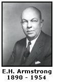
Edwin Howard Armstrong is widely regarded as one of the foremost contributors to the field of radio-electronics.
Among his principal contributions were regenerative feedback circuits, the superheterodyne radio receiver, and a
frequency-modulation radio broadcasting system. It superseded the tuned radio frequency receiver TRF also invented
by Armstrong in 1918. He was inducted into the National Inventors Hall of Fame in 1980.
Armstrong was born on December 18, 1890, in New York City, where he was to spend much of his professional career.
He graduated with a degree in electrical engineering from Columbia University in 1913, and observed the phenomenon of
regenerative feedback in vacuum-tube circuits while still an undergraduate. At Columbia, he came under the influence
of the legendary professor-inventor,
In the early 1930's, the superheterodyne receiver was king.
Edwin Howard Armstrong is widely regarded as one of the foremost contributors to the field of radio-electronics.
Among his principal contributions were regenerative feedback circuits, the superheterodyne radio receiver, and a
frequency-modulation radio broadcasting system. It superseded the tuned radio frequency receiver TRF also invented
by Armstrong in 1918. He was inducted into the National Inventors Hall of Fame in 1980.
Armstrong was born on December 18, 1890, in New York City, where he was to spend much of his professional career.
He graduated with a degree in electrical engineering from Columbia University in 1913, and observed the phenomenon of
regenerative feedback in vacuum-tube circuits while still an undergraduate. At Columbia, he came under the influence
of the legendary professor-inventor, 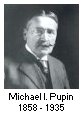 Michael I. Pupin,
who served as a role model for Armstrong and became an effective promoter of the young inventor. In 1915 Armstrong
presented an influential paper on regenerative amplifiers and oscillators to the IRE. Subsequently, regenerative
feedback was incorporated into a comprehensive engineering science developed by Harold Black, Harry Nyquist, Hendrik
Bode, and others in the period between 1915 and 1940.
Michael I. Pupin,
who served as a role model for Armstrong and became an effective promoter of the young inventor. In 1915 Armstrong
presented an influential paper on regenerative amplifiers and oscillators to the IRE. Subsequently, regenerative
feedback was incorporated into a comprehensive engineering science developed by Harold Black, Harry Nyquist, Hendrik
Bode, and others in the period between 1915 and 1940.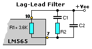
 Although the synchronous, or homodyne, receiver was superior to the superheterodyne method, the cost of a phase-locked
loop circuit outweighed its advantages.
Because of this prohibitive cost the widespread use of this principle did not begin until the development of the
monolithic integrated circuit and incorporation of complete phased-lock loop circuits in low-cost IC packages--
then things started to happen.
Although the synchronous, or homodyne, receiver was superior to the superheterodyne method, the cost of a phase-locked
loop circuit outweighed its advantages.
Because of this prohibitive cost the widespread use of this principle did not begin until the development of the
monolithic integrated circuit and incorporation of complete phased-lock loop circuits in low-cost IC packages--
then things started to happen.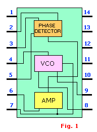
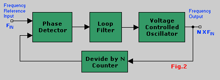
 This is an ideal method for generating clocking pulses at
a multiple of the power-line frequency for integrating A/D
converters (dual-slope, charge-balancing), in order to have infinite rejection of interference at the power-line
frequency and its harmonics. It also provides the basic technique of frequency synthesizers.
This is an ideal method for generating clocking pulses at
a multiple of the power-line frequency for integrating A/D
converters (dual-slope, charge-balancing), in order to have infinite rejection of interference at the power-line
frequency and its harmonics. It also provides the basic technique of frequency synthesizers.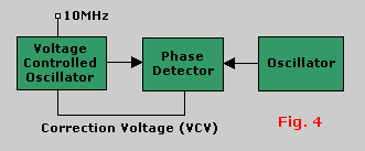 What if we feed the output of a VCO and
Crystal Oscillator into a phase detector? What is a Phase Detector? (See Fig. 4).
It is similar to a discriminator or ratio detector used in frequency demodulation or it could be a digital device,
like an 'Exclusive OR' gate.
What if we feed the output of a VCO and
Crystal Oscillator into a phase detector? What is a Phase Detector? (See Fig. 4).
It is similar to a discriminator or ratio detector used in frequency demodulation or it could be a digital device,
like an 'Exclusive OR' gate.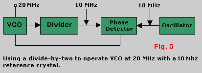 Let's investigate how we can solve this problem. Suppose
our crystal frequency was 10 MHz, but we wanted the VCO to operate on 20 MHz. The phase detector will of course
detect a frequency difference and pull the VCO down to 10 MHz, but what if we could fool the phase detector into
thinking the VCO was really only operating on 10 MHz, when in reality it is operating on 20 MHz. Take a look
at Fig. 5. Suppose, for example in Fig. 4 we used a divide-by-four instead of the
divide-by-two. Then, at LOCK, the VCO would be oscillating at 40 MHz yet still be as stable as the crystal reference
frequency.
Let's investigate how we can solve this problem. Suppose
our crystal frequency was 10 MHz, but we wanted the VCO to operate on 20 MHz. The phase detector will of course
detect a frequency difference and pull the VCO down to 10 MHz, but what if we could fool the phase detector into
thinking the VCO was really only operating on 10 MHz, when in reality it is operating on 20 MHz. Take a look
at Fig. 5. Suppose, for example in Fig. 4 we used a divide-by-four instead of the
divide-by-two. Then, at LOCK, the VCO would be oscillating at 40 MHz yet still be as stable as the crystal reference
frequency.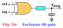 PLL
Components
PLL
Components mixer". Highly linear phase detectors of this type are essential for lock-in detection, which is a fine
technique.
mixer". Highly linear phase detectors of this type are essential for lock-in detection, which is a fine
technique.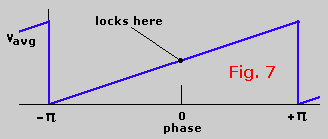 The type II phase detector is sensitive only to the
relative timing of edges between the signal and VCO input, as shown in Fig. 6..
The phase comparator circuit generates either lead or lag output pulses, depending on whether the VCO
output transitions occur before or after the transitions of the reference signal, respectively. The width of these
pulses is equal to the time between the respective edges. The output circuitry then either sinks or sources current
(respectively) during those pulses and is otherwise open-circuited, generating an average output-voltage-versus-phase
difference like that in Fig. 7. This is
completely independent of the duty cycle of the input signals, unlike the situation with the type I phase comparator
discussed earlier. Another nice feature of this phase detector is the fact that the output pulses disappear entirely
when the two signals are in lock. This means that there is no "ripple" present at the output to generate periodic
phase modulation in the loop, as there is with the type I phase detector. Also, there is an additional difference
between the two kinds phase detectors. The type I detector is always generating an output wave, which must then be
filtered by the loop filter. Thus, in a PLL with type I phase detector, the loop filter acts as a low-pass filter,
smoothing this full-swing logic-output signal. There will always be residual ripple, and consequent periodic phase
variations, in such a loop. In circuits where phase-locked loops are used for frequency multiplication or synthesis,
this adds "phase-modulation sidebands" to the output signal.
The type II phase detector is sensitive only to the
relative timing of edges between the signal and VCO input, as shown in Fig. 6..
The phase comparator circuit generates either lead or lag output pulses, depending on whether the VCO
output transitions occur before or after the transitions of the reference signal, respectively. The width of these
pulses is equal to the time between the respective edges. The output circuitry then either sinks or sources current
(respectively) during those pulses and is otherwise open-circuited, generating an average output-voltage-versus-phase
difference like that in Fig. 7. This is
completely independent of the duty cycle of the input signals, unlike the situation with the type I phase comparator
discussed earlier. Another nice feature of this phase detector is the fact that the output pulses disappear entirely
when the two signals are in lock. This means that there is no "ripple" present at the output to generate periodic
phase modulation in the loop, as there is with the type I phase detector. Also, there is an additional difference
between the two kinds phase detectors. The type I detector is always generating an output wave, which must then be
filtered by the loop filter. Thus, in a PLL with type I phase detector, the loop filter acts as a low-pass filter,
smoothing this full-swing logic-output signal. There will always be residual ripple, and consequent periodic phase
variations, in such a loop. In circuits where phase-locked loops are used for frequency multiplication or synthesis,
this adds "phase-modulation sidebands" to the output signal.