Photosensitive Devices
"Learn to use photoconductive cells, photodiodes, and phototransistors in practical light controlled circuits."
© Ray M. Marston, Tony van Roon
We will look at Light-Sensitive devices in this article and find out how they can be used in various practical control circuits. Light-sensitive
devices include photocells, photodiodes, and phototransistors. Visible and infrared light (or the absence of that light) can trigger many different
kinds of circuit for the control of alarms, lights, motors, relays, and other actuators. Light-sensitive devices, sometimes called photoelectric
transducers, alter their electrical characteristics in the presence of visible or infrared light.
 Photocell Basics:
Photocells are also called by many other names including photoconductive cells, light-dependent resistors (LDR's), and photoresistors. They are
variable resistors with an extremely wide range of resistance values (up to hundreds of orders of magnitude) that are dependent on the level of
incident light. Resistance in photocells varies inversely with the strength of light that falls on them. In other words, resistance is very high in
the dark, but low under bright light.
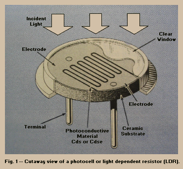
Figure 1 is a cutaway view of a typical photocell showing the pattern of photoconductive material deposited in the
serpentine slot separating the two electrodes that have been formed on a ceramic insulating substrate. This pattern maximizes contact between the
crystalline photoconductive material and the adjacent metal electrodes.
The photoconductive material is typically Cadmium Sulfide (CdS) or Cadmium Selenide (CdSe). The selection of the material and the thickness and
width of its deposition determine the resistance value and power rating of the device. The two-terminal assembly is enclosed in a metal or opaque
plastic case with a clear glass or plastic window over the photo-conductive material. Newer types just uses a very hard clear lacquer coating on a
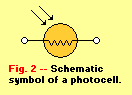
very thin wafer. Figure 2 is the schematic symbol for the photocell.
 Photocells are made with diameters from about one-eight inch (3mm) to over one inch (25mm); the most popular devices have diameters of about three-eight
inch (10mm). The smaller units are suitable for applications where space is limited, such as in card-reading applications (which method is no longer
used I think), but they have low-power dissipation ratings. Another application is a so-called 'sun-tracker' used to keep large solar panels in the
sun. Some photocells are hermetically sealed to withstand the effects of demanding environments.
Photocells are made with diameters from about one-eight inch (3mm) to over one inch (25mm); the most popular devices have diameters of about three-eight
inch (10mm). The smaller units are suitable for applications where space is limited, such as in card-reading applications (which method is no longer
used I think), but they have low-power dissipation ratings. Another application is a so-called 'sun-tracker' used to keep large solar panels in the
sun. Some photocells are hermetically sealed to withstand the effects of demanding environments.
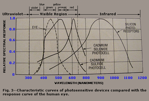
Figure 3 compares the response of photosensitivity devices characteristics with that of the human eye. Relative spectral
response is plotted against wavelength from 300 to 1200 nanometers (nm). The bell-shaped human eye response curve shows that the eye is sensitive to
a relatively narrow band of the electromagnetic spectrum, between 400 and 750 nm. The curve peaks in the green light region at about 550nm and extends
down into the violet region (400 to 450nm) at one end, and up into the dark red light region (700 to 780nm) at the other end.
 Also, Figure 3 shows why cadmium sulfide (CdS) photocells are so popular for light-controlled circuits; the CdS spectral
response curve peaks near 600nm, and it closely matches that of the human eye. By contrast, the response curve for Cadmium Selenide (CdSe) peaks
further out at about 720nm. However, CdSe is also sensitive to most of the visible-light region.
Also, Figure 3 shows why cadmium sulfide (CdS) photocells are so popular for light-controlled circuits; the CdS spectral
response curve peaks near 600nm, and it closely matches that of the human eye. By contrast, the response curve for Cadmium Selenide (CdSe) peaks
further out at about 720nm. However, CdSe is also sensitive to most of the visible-light region.
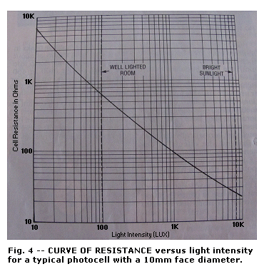
A typical CdS photocell characteristic curve is shown in Fig. 4. Its dark resistance is about five mega-ohms. This
value falls to about 600 ohms at a light intensity of 100 lux, typical of a well illuminated room and to about 30 ohms at an intensity of 8000 lux,
typical of bright sunlight. (The lux is the SI unit of illuminance produced by a luminous flux of 1 lumen uniformly distributed over a surface of
1 square meter).
Commercial photocells have good power and voltage ratings, similar to those of conventional resistors. Power dissipation ratings could be between 50
and 500 milliwatts, depending on detector material. Their only significant drawbacks are their slow response times. Cadmium Selenide photocells
generally have shorter time constants than Cadmium Sulfide photocells (approximately 10 milliseconds versus 100 milliseconds). They also offer lower
resistance values, higher sensitivities, and higher temperature coefficients of resistance.
Photocells are included in photographic exposure meters, light-and dark-activated lights, and intrusion alarms. Some light-activated alarms are
 triggered by breaking a light beam. There are even light-reflective smoke alarms based on photocells. Fig. 5 to 20 show
practical photocell circuits; each will work with almost any photocell.
triggered by breaking a light beam. There are even light-reflective smoke alarms based on photocells. Fig. 5 to 20 show
practical photocell circuits; each will work with almost any photocell.
Photocell Light Switches:
Fig. 5 to 10 illustrate practical light-activated switch circuits with relay contact outputs that are based on the photocell.
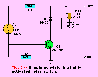
The simple circuit shown in Fig. 5 is designed to react when light enters a normally dark space such as the inside of a
cabinet or closet. The photocell R3 and resistor R2 form a voltage divider that sets the base bias of Q1. Under dark conditions, the photocell has a
high resistance, so zero bias is applied to the base of Q1; in this state, Q1 and the relay RY1are off. when a sufficient amount of light falls on the
photocell, its resistance drops to a low value, and bias is applied to the base of Q1. That bias activates RY1, and its contacts can control external
circuitry.
The simple Fig. 5 circuit has low sensitivity and no provision for sensitivity adjustment. Fig. 6
illustrates how these drawbacks can be overcome with Darling-coupled transistors Q1 and Q2 replacing Q1, and the use of a potentiometer R2 for sensitivity
control, replacing fixed resistor R2. The diagram also shows how the circuit can be made self-latching with the second set of relay contacts.
Normally-closed (NC) pushbutton switch S1 permits the circuit to be reset (unlatched) when required.
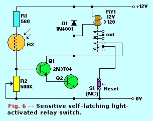
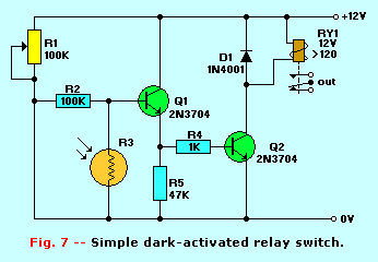
Figure 7 shows how a photocell can form a simple dark-activated relay that turns on when the light level falls below a value
preset by potentiometer R1. Resistor R2 and the photocell R3 form a voltage divider. The voltage at the R2-R3 junction increases with falling light.
That voltage, buffered by emitter-follower Q1, controls relay RY1 with common-emitter amplifier Q2 and current-limiting resistor R4.
The light trigger or threshold levels of the circuits shown in Fig. 6 and 7 are susceptible to variations in supply voltage
and ambient temperature. Figure 8 shows a very sensitive precision light-activated circuit that is not influenced by
those variables. In this circuit the photocell R5, potentiometer R6, and resistors R1 and R2 are connected to form a Wheatstone Bridge, and op-amp
IC1 and the combination of transistor Q1 and RY1 act as a highly sensitive balance-detecting switch. The bridge balance point is independent of
variations in supply voltage and temperature, and is influenced only by variations in the relative values of the bridge components.
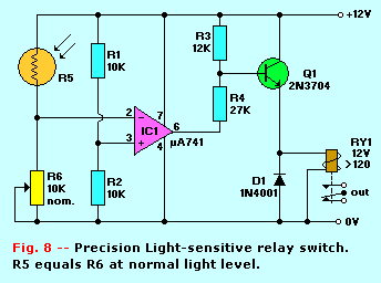
In Fig. 8, the photocell R5 and potentiometer R6 form one arm of the bridge, and R1 and R2 form the other arm. Those
arms can be considered as voltage dividers. The R1-R2 arm applies a fixed half-supply voltage to the non-inverting input of the op-amp, while the
photocell-potentiometer divider applies a light-dependent variable voltage to the inverting pin of the op-amp.
To use this circuit, potentiometer R6 is adjusted so that the voltage across the photocell and the potentiometer rises fractionally above that across
R1 and R2 as the light intensity rises to the desired trigger level. Under that condition, the op-amp output switches to negative saturation, which
turns on Q1 and thus RY1. When the light intensity falls below that level, the op-amp output switches to positive saturation, and Q1 and the relay are
turned off.
The circuit in In Fig. 8 is so sensitive that it is able to respond to changes in light-level that are too small to be
detected by the human eye. The circuit can be modified to act as a precision dark-activated switch by either transposing the inverting and
non-inverting input pins of the op-amp, or by transposing the photocell and the adjacent potentiometer.
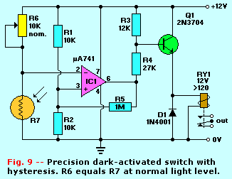
The circuit in In Fig. 9 also shows how a small amount of hysteresis can be added to the circuit with the feedback
resistor R5 so hat relay RY1 is actuated when the light level falls to a preset value. However, the relay is not de-actuated again until the light
intensity increases substantially about that value. The hysteresis magnitude is inversely proportional to the value of R5, but is zero when R5 is
open circuited.
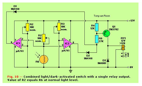
Figure 10 shows how a precision light/dark switch can be made by combining op-amp light and dark switches. The switch
activates relay RY1 if the light intensity rises above one preset value or falls below another preset value. Potentiometer R1 controls the dark
level, potentiometer R2 controls the supply voltage, and potentiometer R3 controls the light level.
To organize the circuit shown in Fig. 10, first preset potentiometer R2 so that about half the supply voltage appears at
the junction between R6 and potentiometer R2 when the photocell is illuminated at its normal intensity level. Potentiometer R1 can then be preset so
that RY1 is actuated when the light intensity falls to the desired dark level and potentiometer R3 can be adjusted so that RY1 is actuated at the
desired brightness level.
In the circuits shown in Fig. 8 to 10, the resistance values of the series potentiometers should equal the photocell's
resistance values at the normal light level of each circuit.
Bell-Output Photocell Alarms:
The light-activated photocell circuits in Figs. 5 to 10 all have relay outputs that can control many different kinds of
external circuits. In many light-activated circuit applications, however, the circuits must trigger audible alarms. This response can also be
obtained without relays as shown in Figs. 11 to 17.
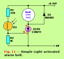
Fig. 11 shows a simple light-activated alarm circuit with a direct output to an alarm buzzer or bell. The bell or buzzer
must be self-interrupting and have an operating current rating less than 2 amperes. The supply voltage should be 1.5 to 2 volts greater than the
nominal operating value of the bell or buzzer. Photocell R3 and resistor R2 form a voltage divider. Under dark conditions, the photocell resistance
is high. so the voltage at the junction R3 and R2 is too small to activate the gate of the silicon-controlled rectifier SCR1. Under bright light
conditions with the photocell resistance low, gate bias is applied to the SCR which turns on and activates the alarm.
In the circuit of Fig. 11, keep in mind that although the SCR is self-latching, the fact that the alarm is
self-interrupting ensures that the SCR repeatedly unlatches automatically as the alarm sounds. (The SCR anode current falls to zero in each
self-interrupting phase.) Consequently, the alarm automatically turns off again when the light level falls below the circuit's threshold level.
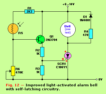
The circuit of Fig. 11 has fairly low sensitivity and no sensitivity adjustment. Figure 12
shows how that drawback can be overcome: potentiometer R6 replaces a fixed resistor and Q1 is inserted as a buffer between photocell R5 and the SCR1
gate. The diagram also shows how to make the circuit self-latching by wiring R4 in parallel with the alarm so the SCR anode current remains above
zero as the alarm self-interrupts. Switch S1 permits the circuit to be reset (un-latched) when required.
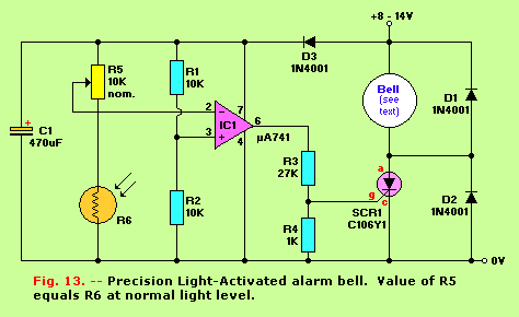 Figure 13 shows how to make a precision light-alarm with an SCR-actuated output based on a Wheatstone Bridge formed by
the photocell R6, potentiometer R5, and op-amp IC1. The op-amp balance detector provides precision control. That circuit can be converted into a
dark-activated alarm by simply transposing the photocell and potentiometer. Hysteresis can also be added, if required.
Figure 13 shows how to make a precision light-alarm with an SCR-actuated output based on a Wheatstone Bridge formed by
the photocell R6, potentiometer R5, and op-amp IC1. The op-amp balance detector provides precision control. That circuit can be converted into a
dark-activated alarm by simply transposing the photocell and potentiometer. Hysteresis can also be added, if required.
Speaker-output Alarms:
Figures 14 to 17 show different ways of using CMOS 4001B quad 2-input NOR-gate IC's to make light-activated alarms that
generate audible outputs with loud speakers. The 4001B is available at the CD4001B from Harris and Motorola, National Semiconductor, Signetics, and
others under various designations that include 4001B.
The circuit of Fig. 14 is a dark-activated alarm circuit that generates a low-power 800Hz pulsed-tone signal at the
speaker.
NOR gates IC1-c and IC1-d are wired as an 800Hz astable multivibrator that can feed tone signals into the speaker from Q1. It is gated on only when
the output of IC1-b is low. NOR gates IC1-a and IC1-b are wired as a 6Hz astable circuit that is gated on only when its gate pin 1 is pulled low.
(Pin 1 is coupled to the voltage divider formed by photocell R4 and potentiometer R5.)
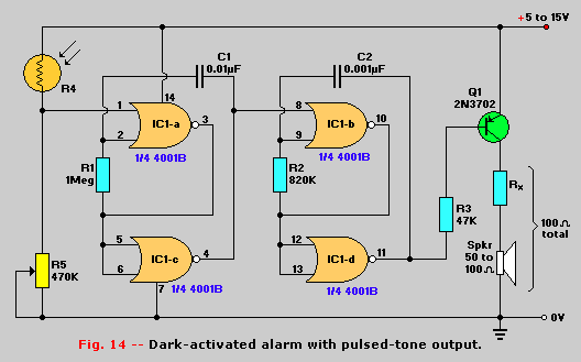 The action of the circuit is as follows: under bright light conditions, the voltage at the junction of the photocell R4 and potentiometer R5 voltage is
high, so both astable circuits are disabled and no output is generated at the speaker. Under dark conditions, the photocell-potentiometer junction
voltage is low, so the 6Hz astable circuit is activated, gating the 800Hz astable on and off at a 6Hz rate. As a result, a signal from Q1 produces a
pulsed-tone in the speaker.
The action of the circuit is as follows: under bright light conditions, the voltage at the junction of the photocell R4 and potentiometer R5 voltage is
high, so both astable circuits are disabled and no output is generated at the speaker. Under dark conditions, the photocell-potentiometer junction
voltage is low, so the 6Hz astable circuit is activated, gating the 800Hz astable on and off at a 6Hz rate. As a result, a signal from Q1 produces a
pulsed-tone in the speaker.
The precise gating level of the 4001B IC is determined by its threshold voltage value, which is a fraction of the supply voltage--nominally 50%.
That value might vary from 30% to 70% in individual devices, but gating points of these IC's are generally stable.
The Fig. 14 circuit provides sensitive dark-activated alarm triggering.
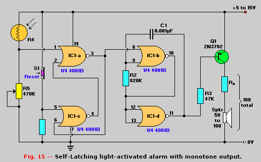 Figure 15 is a schematic of a self-latching light-activated alarm with an 800Hz monotone output. In this circuit, IC1-c
and IC1-d are also wired as a gated 800Hz astable circuit, but IC1-a and IC1-b are wired as a bistable multivibrator with a normally high output.
Under bright light conditions, the photocell-potentiometer junction goes high and latches the bistable circuit into its alternate state. As a result,
the 800Hz astable circuit is gated on to generate the monotone alarm signal. The circuit remains in that state until dark conditions return, and the
bistable circuit is simultaneously reset with S1
Figure 15 is a schematic of a self-latching light-activated alarm with an 800Hz monotone output. In this circuit, IC1-c
and IC1-d are also wired as a gated 800Hz astable circuit, but IC1-a and IC1-b are wired as a bistable multivibrator with a normally high output.
Under bright light conditions, the photocell-potentiometer junction goes high and latches the bistable circuit into its alternate state. As a result,
the 800Hz astable circuit is gated on to generate the monotone alarm signal. The circuit remains in that state until dark conditions return, and the
bistable circuit is simultaneously reset with S1
 The light/dark operation of the circuits in Figs. 14 and 15 can be reversed by transposing the photocell and potentiometer.
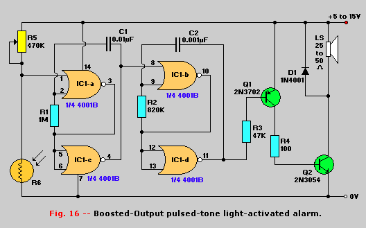
Each circuit produces only a few milliwatts of output power. Figure 16 shows how the operation of the
dark-operated circuit of Fig. 14 can be reversed to become light-operated by switching the positions of the photocell and
potentiometer. The output power can be boosted with an additional output transistor Q2. This circuit can operate from a 5 to 15volt supply and with
25 to 50 ohm loud-speaker. The output power can vary from 0.25 to 11.25 watts, depending on the voltage and impedance values.
The light/dark operation of the circuits in Figs. 14 and 15 can be reversed by transposing the photocell and potentiometer.
Each circuit produces only a few milliwatts of output power. Figure 16 shows how the operation of the
dark-operated circuit of Fig. 14 can be reversed to become light-operated by switching the positions of the photocell and
potentiometer. The output power can be boosted with an additional output transistor Q2. This circuit can operate from a 5 to 15volt supply and with
25 to 50 ohm loud-speaker. The output power can vary from 0.25 to 11.25 watts, depending on the voltage and impedance values.
The circuits shown in Fig. 14 to 16 have adequate sensitivity levels for most practical applications. However, if
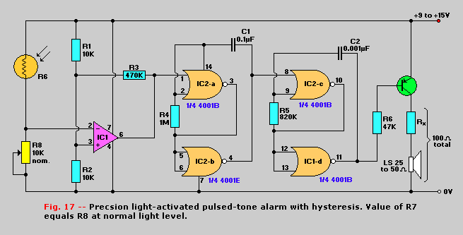
required, both sensitivity and trigger-level stability can be increased. That's done in Fig. 17 by inserting an op-amp
between the voltage divider junction formed by photocell R7 and potentiometer R8 and gate pin 1 of IC2-a. Resistor R3 controls the hysteresis of the
circuit, but it can be removed if hysteresis is not needed.
Selection of Photocell Circuits:
Photocells are widely used in alarms that triggered by interrupting a visible light beam. They are (were) used in smoke-alarms that are actuated when
smoke particles reflect light back to the photocell. Figures 18 to 20 show self-interrupting alarm-bell versions of those
warning circuits.
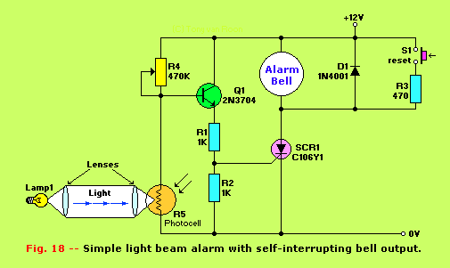
The interrupted light beam activated alarm circuit of Fig. 18 acts like a dark-operated alarm. Normally, the photocell
is illuminated by the light beam so its resistance is low and only low voltage appears at the junction of potentiometer R4 and photocell R5.
Consequently, both the SCR and bell are off. When the light beam is broken, photocell resistance increases and a significantly higher voltage appears
at the potentiometer-photocell junction. Under this condition SCR1 conducts and the alarm bell rings. Resistor R3 in series with switch S1
self-latches the alarm.
Figure 19 is a cutaway view of a reflective-type smoke detector. The lamp and photocell are mounted on one wall of the
box whose open ends are covered with lids mounted on spacers. The openings provided by the spacers permit smoke to pass through the detector while
ambient light is excluded. An internal baffle prevents incandescent lamp light from falling directly on the photocell.
The lamp acts as both a source of light and heat; the heated air in the box rises, creating air convection currents that draw air in at the bottom of
the box and expel it from the top. The inside of the box is painted matte black to eliminate reflections.
If the air currents moving through the detector box are free of smoke, no light will fall on the photocell, and its resistance will be very high.
However, if the air contains smoke, the particulates of tat smoke reflect light from the lamp back onto the photocell face, causing its resistance to
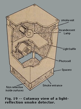 decrease sharply. That resistance drop can trigger an alarm. Figure 12 is a practical control circuit that can be used
in the smoke alarm shown in Fig. 19.
decrease sharply. That resistance drop can trigger an alarm. Figure 12 is a practical control circuit that can be used
in the smoke alarm shown in Fig. 19.
Photodiodes Put to Use:
If a conventional silicon diode is connected in the reverse-biased circuit of Fig. 20, only leakage current will flow
through the diode and no voltage will be developed across resistor R1. However, if the case is removed from a conventional silicon diode to expose
its PN junction, and the diode is then replaced in the same circuit, its photosensitive properties can be observed.
When the diode is exposed to light, its current could rise to as much as on milliampere, producing a voltage across R1. All silicon PN junctions are
photosensitive. Thus a photodiode is essentially a conventional silicon PN-junction diode in a case with a transparent cover to permit light to reach
its junction. Figure 21 shows its standard schematic symbol.
In Fig. 22 the photodiode is reverse biased and its output voltage is taken across a series connected load resistor R1.
That resistor could also be connected between the diode and ground as shown in Fig. 20. Photodiodes also have spectral
response characteristics, which are determined by the doping of the semiconductor material.
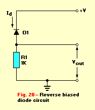
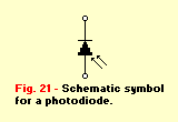
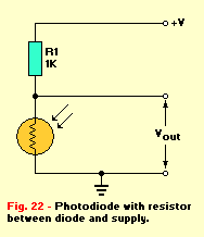
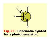 Figure 3 shows a typical response curve that applies for all silicon photoreceptors, a category which includes both
photodiodes and phototransistors. While silicon photodiodes have lower visible-light sensitivity than either cadmium-sulphide or cadmium-selenide
photocells, they respond faster to changes in light level. As stated earlier, cadmium-sulphide and cadmium-selenide photocells are best suited for
applications in visible light in which they are directly couple and where relatively slow response time is acceptable. By contrast, photodiodes are
better suited for application sin the infrared region in which they receive AC signals and where fast response is required.
Figure 3 shows a typical response curve that applies for all silicon photoreceptors, a category which includes both
photodiodes and phototransistors. While silicon photodiodes have lower visible-light sensitivity than either cadmium-sulphide or cadmium-selenide
photocells, they respond faster to changes in light level. As stated earlier, cadmium-sulphide and cadmium-selenide photocells are best suited for
applications in visible light in which they are directly couple and where relatively slow response time is acceptable. By contrast, photodiodes are
better suited for application sin the infrared region in which they receive AC signals and where fast response is required.
Photodiodes are typically used in infrared remote-control circuits, beam interruption switches and alarm circuits. However, lead-sulphide (PbS)
photocells have characteristics that are similar to those of visible light photocells except that they function only in the infrared region.
 Phototransistors:
Figure 23 shows the standard phototransistor symbol. The phototransistor is a silicon bipolar NPN transistor in a case
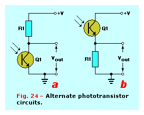
with a transparent cover (or lens) that allows light to reach its PN junctions. The device is normally used with its base pin open-circuited as
shown in both parts of Fig. 24. In Fig. 24a, the base-collector junction of the
phototransistor is effectively reversed biased so it acts as a photodiode. The light-generated currents of the base-collector junction feed directly
into the base of the device, and the normal current-amplifications of the transistor causes collector current to flow as the output. That amplified
current across R1 produces the output voltage.
Phototransistor collector and emitter currents are usually similar because the base connection is open circuited, and the device is not subjected to
negative feedback. As a consequence, the alternative circuit shown in Fig 24b offers about the same performance
as the shown in Fig 24a. The output voltage appears across R1 which is connected between the emitter and ground.
The sensitivity of a phototransistor is typically one hundred times greater than that of a photodiode. However, its useful maximum operating frequency
of a few hundred kilohertz is proportionally lower than that of a photodiode's tens of megahertz. A phototransistor can be converted into a photodiode
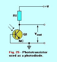
by connecting it as shown in Fig 25.
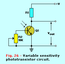
Alternatively, the sensitivity and operating speed of a phototransistor can be made variable by wiring a potentiometer between its base and emitter,
as shown in Fig 26. With R2 open circuited, phototransistor operation is obtained; with R2 short circuited, a photodiode
response occurs.
In practical applications of the circuits shown in Fig 24 through 26, the R1 load value is usually selected as a compromise
because voltage gain increases but the useful operating bandwidth decreases with the value of R1. Also, the value of R1 must, in many applications, be
chosen to bring the photosensitive device into its linear operating region.
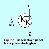
Darlington phototransistors consist of two transistors coupled as shown in the schematic symbol of Fig. 27.
Typical sensitivities of the photo-darlingtons are about then times greater than those of standard phototransistors, but their useful maximum
operating frequencies are only tens of KiloHertz.
Pre-amplifier Circuits:
Photodiodes and phototransistors are used as lightwave signal receivers or detectors in fiber optic transmission lines. The light traveling in the
optical fiber can be modulated by either analog or digital methods. Photodiodes and phototransistors are also detectors in optocouplers and infrared
light-beam interruption switching and alarm-control systems.
In those applications, the signal reaching the photosensor could either be very strong or very weak. Moreover, the photosensor could be subjected to
a lot of noise in the form of random, unwanted visible or infrared emissions. To minimize interference problems, optical links are usually operated in
the infrared range, and the optosensor's output is then processed with a low-noise preamplifier having a wide dynamic operating range.
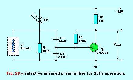
Figures 28 and 29 illustrate typical examples of preamplifier circuits with photodiode sensors.
The Fig. 28 circuit is designed for use with a 30KHz carrier. The tuned circuit, consisting of L1, C1, and C2, is wired
in series with D1 and damped by R1 to provide the necessary frequency-selective low-noise response. The output signals are tapped off at the junction
between C1 and C1 and then amplified by Q1.
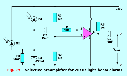
The 20KHz selective preamplifier shown in Fig. 29 is intended for an infrared light-beam alarm. The alarm sounds when the
beam is broken. Two IR photodiodes, D1 and D2, are wired in parallel so that the optical signals are lost only when both photodiode signals are cut
off. Register R1 is shunted by C1 to reject unwanted high-frequency signals. The output signals across R1 are fed to the inverting op-amp through
C2, which rejects unwanted low-frequency signals.
Suggested Reading:
"The Way Things Work", by David Macaulay
"Physics for Scientists and Engineers", by Paul Fishbane, Stephen Gasiorowicz, and Stephen Thornton
"Feynman's Lectures on Physics", by Richard Feynman
Copyright and Credits:
Ray M. Marston, "Photosensitive Devices", Electronics Now magazine, July 1992.
Tony van Roon, editor, graphics and photos, newly edited material, September 2010.
(Hugo) Gernsback Publishing is (sadly) out of business since 2000.
Re-posting or taking graphics in any way or form from this website or of this project is expressly prohibited by
international copyright © laws. Permission by written permission only.
Copyright © 2010 - Tony van Roon, VA3AVR
Last updated: October 14, 2010