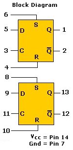
MC14013B Dual Type D Flip-FLop
Data sheet
Direct substitute for CD4013B
by Tony van Roon
The MC14013B dual type D flip-flop is constructed with MOS P-Channel enhancement mode devides in a single monolithic
structure. Each flip-flop has independent Data, (D), Direct Set, (S), Direct Reset, (R), and Clock, (C), inputs and
complementary outputs (Q and Q-not). These devices may be used as shift-register elements or as type 'T' flip-flops
for counter and toggle applications. The MC14013B CMOS SSI is a low-power complimentary MOS.
This device contains protection circuitry to guard against damage due to high static voltage or electric fields. However,
precautions must be taken to avoid applications of any voltage higher than the maximum rated voltages to this high-impedance
circuit. For proper operation, Vin and Vout should be constrained to the range Vss [much-smaller-than] (Vin or Vout)
[much-smaller-than] Gnd. Unused inputs must
always be tied to an appropriate logic voltage level (e.g. either Vcc or Gnd). Unused outputs
must be left open.
 Notes:
DC Supply Voltage range (Vcc) 3 to 18 volt.
Static operation.
Diode protection on All inputs.
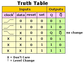
Logic Edge-Clocked flip-flop design -- Logic state is retained indefinately with clock level either high or low;
information is transferred to the output only on the positive going edge of the clock pulse.
Capable of driving two Low-power TTL loads or one Low-power Shottky TTL load over the rated temperature range.
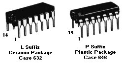
Pin-for-Pin Replacement for the CD4013B.
Storage Temperature range from -65 °C to +150 °C.
Power dissipation 500mWatt.
Lead temperature 260 °C (Maximum 8 seconds per leg for soldering).
Maximum rating (Vcc) 0.5v to 18v. (Voltages referenced to Gnd)
Input or Output Voltage (DC or Transient) 0.5 to Vdd +0.5.
Input or Output Current (DC or Transient), per Pin; Plus or Minus 10mA.
![[pins]](mc14013d.jpg)
![[1/2 Logic Diagram]](mc14013e.jpg)
Back to Circuits or Gadgets page
Copyright © 1996 - Tony van Roon