"Build these circuits that can amplify, filter, generate white noise,
flash lamps, locate hidden metal--and perhaps even detect lies."
Rewritten by Tony van Roon
This last article on bipolar junction transistors (BJT) is a potpourri of circuits. Some are practical and some are
not so practical, but they can be great for experiments. With these circuits you can amplify signals, filter high
and low frequencies, generate white noise, and flash lamps. You can also boost DC voltage levels, locate hidden metal
objects, and detect rising water. One circuit will even demonstrate the fundamentals of lie detection!
More Power Amplifiers:
Today the easiest way to build a low- to medium-power audio amplifier is to pick an integrated circuit (IC) amplifier
from a manufacturer's data book and supplement it with additional components recommended in the applications notes in
the data book. However, if you just want to learn amplifier principles by experimentation or you have a simple
application in mind, you should build the amplifier with discrete transistors.
Figure 1 is a schematic for a general-purpose, low-power, high-gain amplifier based on
discrete transistors. A Class-A amplifier, it can drive a load such as a speaker or headset with an impedance greater
than 65 ohms. The amplifier draws a quiescent current of about 20 milliamperes. However, this drain can be reduced by
increasing the value of R3.
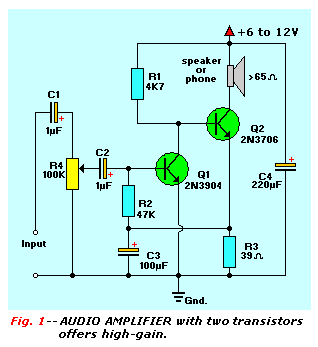
Transistors Q1 and Q2 are configured as common-emitter amplifiers; the output of Q1 is directly coupled to the input
of Q2. This circuit has an overall voltage gain of about 80 dB. Notice that resistor R3, the emitter load of Q2, is
decoupled by capacitor C3 so that the Q2 emitter follows the average collector voltage of Q1.
The base bias for Q1 is derived from Q2's emitter through R2. With this configuration, the bias is stabilized by
negative DC feedback. Input potentiometer R4 serves as the circuit's volume control.
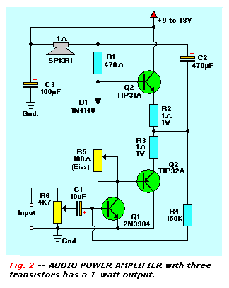
Figure 2 is the schematic for a simple, three-transistor, Class-AB complementary amplifier
which can drive about 1 Watt into a 3-ohm speaker load. Transistor Q1, which is configured as a common-emitter
amplifier, drives a load that is the sum of speaker SPKR1. resistor R1 and potentiometer R5. Its output voltage is
followed and boosted in power by the complementary emitter-follower stage made up of Q2 and Q3.
The output of the amplifier is fed through capacitor C2 to the junction of SPKR1 and R1 where it provides a
low-impedance drive for SPKR1. It simultaneously bootstraps the value of R1 so that the circuit has high-voltage gain.
The output is also fed back to Q1's base through R4 so that it produces a base bias through a negative feedback loop.
Carefully adjust trimmer potentiometer R5 to minimize audible signal crossover distortion so that it is consistent with
lowest quiescent current consumption that can be measured. To obtain a reasonable value, set the quiescent current
from 10 to 15 milliamperes.
Figure 3 shows a more complex audio power amplifier that can deliver about 10 watts into a
8-ohm load when powered from a 30-volt supply. This circuit includes four, high-gain, quasi-complementary output stage
(Q3 to Q6). Transistor Q1 functions as an adjustable amplifier diode output biasing device in this circuit.
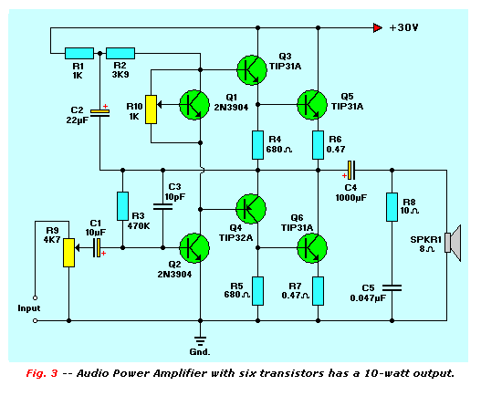
The main load resistor R2 of the Q2 common-emitter amplifier stage is bootstrapped by C2 and DC biased by R3. This
network should set the quiescent output voltage at about half the power supply value. If it does not, alter the value
of R3. The upper frequency response of the amplifier is restricted by C3, which menaces circuit stability. In
addition, capacitor C5 is wired in series with R8 across the output of the amplifier to increase circuit stability.
The amplifier should be set up initially as was described for the circuit in Fig. 2.
Scratch/Rumble Filters:
Today, with the widespread acceptance of compact discs (CDs/DVDs), records (LP) are long obsolete. However, because of
the everlasting popularity of the record (it seems), the last couple years manufacturers have been bringing back the
old record player in a new coat. Like myself, many people still own a large collection of these records, and when
played on quality record players, they can still provide many hours of listening pleasure.
Back when the records were popular, unless the record player amplifiers were properly filtered, scratch and rumble noise
could interfere with reception. This interference was even more evident in the playing of the old 78 rpm records, you
know, the old hard and fragile bakelite kind. While scratch and rumble are no longer universal problems, the techniques
for eliminating them are still interesting.
Scratch noise is essentially sound at a frequency greater than 10KHz picked up from the record's surface, while
rumble is sound at a frequency typically less than 50 Hz caused by variations in turntable drive motor speed.
Each of these noises can be effectively eliminated or attenuated by passing the audio output from the record player
through a filter that rejects the annoying parts of the audio spectrum.
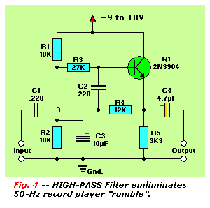
 The rumble filter in Fig. 4 is a high-pass filter that provides unity voltage gain for
all frequencies greater than 50Hz. however, it provides 12 dB per octave rejection to all frequencies below 50Hz.
For example, attenuation is 40dB at 5Hz. Transistor Q1 is configured as an emitter-follower biased at about half the
supply value from the low-impedance junction formed by R1 and R2 in parallel with capacitor C3.
The rumble filter in Fig. 4 is a high-pass filter that provides unity voltage gain for
all frequencies greater than 50Hz. however, it provides 12 dB per octave rejection to all frequencies below 50Hz.
For example, attenuation is 40dB at 5Hz. Transistor Q1 is configured as an emitter-follower biased at about half the
supply value from the low-impedance junction formed by R1 and R2 in parallel with capacitor C3.
However, negative feedback applied through the filter network of R3, C2, C1, and R4 causes an active filter
response. The rolloff frequency of the circuit can be altered, if desired, by changing the values of capacitors C1
and C2--provided that they are kept equal. For example, if the values of C1 and C2 are reduced 50% from 0.220 to
0.110 microfarads, the rolloff frequency will be double to 100Hz.
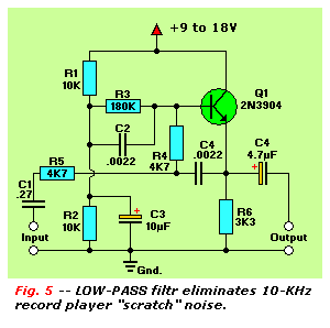
The scratch filter circuit in Fig. 5 acts as a low-pass filter that provides unity voltage
gain to all frequencies below 10KHz, but it rejects all frequencies above 10 KHz at 12dB per octave. This circuit
resembles Fig. 4 except that the positions of the resistors and capacitors are transposed
in the network consisting of C2, R4, C4, and R5.
The rolloff frequency of that circuit can be altered, if desired, by changing the values of C2 and C4. For example,
if both are increase from 0.0022 microfarads to 0.0033microfards, the rolloff frequency is reduced from 10KHz to 7.5KHz.
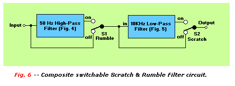
The circuits of Fig. 4 and 5 can be combined to make a composite scratch and rumble filter.
The output of the high-pass filter is connected to the input of the low-pass filter. If desired, bypass switches can
be installed in the individual filter sections so that the filters can easily be switched in and out of circuit. This
change is illustrated schematically in Fig. 6.
It's worth noting that if the circuits of Fig. 4 and 5 are built on a single board, three
components can be saved by making the biasing network composed of resistors R1 and R2 and capacitor C3 common to both
filter circuits.
 Noise Circuits:
White Noise is a steady hissing sound obtained by mixing a full spectrum of randomly generated audio frequencies,
each having equal sound power when averaged over time. White noise can be heard by tuning an FM radio receiver to that
part of the band where no nearby station can be heard. It is intentionally generated for testing audio- and
radio-frequency amplifiers. It can also be an effective sleep aid because it masks random background noises from
voices, passing vehicles, car horns, closing doors, and other sources.
Figure 7-a is the schematic for a simple but useful white noise generator base on the
inherent white-noise generation capability of a revers-biased zener diode. In this circuit, resistor R2 and zener
diode D1 form a negative-feedback loop between the collector and base of common-emitter amplifier Q1.
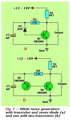 This loop stabilizes the DC working levels of the circuit, and capacitor C1 decouples the AC. As a result, D1
becomes a white-noise source in series with the case of Q1, which amplifiers that noise to a useful level of about
1 volt, peak-to-peak.
This loop stabilizes the DC working levels of the circuit, and capacitor C1 decouples the AC. As a result, D1
becomes a white-noise source in series with the case of Q1, which amplifiers that noise to a useful level of about
1 volt, peak-to-peak.
The base-emitter junction of any silicone transistor can function as a noise-generating zener diode if its junction is
reverse-biased to tits breakdown level. This breakdown typically occurs in a 2N3904 small-signal BJT at about 6 volts.
Figure 7-b shows the schematic of a two-transistor, white-noise generator. In this
circuit Q1 acts as a zener diode.
Audio noise can be annoying, especially if you are trying to listen to a very weak broadcast station. You might find
that the peaks of unwanted background noise completely swamp the broadcast signal, making it unintelligible. It is
possible to overcome this problem with the noise-limiter circuit shown in Fig. 8.
In this circuit, both the signal and the noise are fed to amplifier Q1 through potentiometer R3. Transistor Q1
amplifies both waveforms equally, but diodes D1 and D2 automatically limit the peak-to-peak output swing of Q1 to
about 1.2 volts. If R3 is adjusted so that the signal output is amplified to this peak level, the noise peaks will
not exceed signal output. Therefore, the receiver signal will be far more intelligible.
Astable Multivibrators:
The astable multivibrator or square-wave generator circuit is versatile. Figure 9, for
example, shows how it can flash two light-emitting diodes (Led) about once per second. Its flash rate is controlled by
the time constant values of resistive-capacitive combinations of R4 and C1 and R3 and C2.
The Leds are in series with the collectors of transistors Q1 and Q2, and they flash on and off symmetrically
out-of-phase with each other. The flash rate can be changed by altering the values of either R4 and C1 or R3 and C2.
You can also replace one of the Leds with a short circuit to make a one-Led flasher.
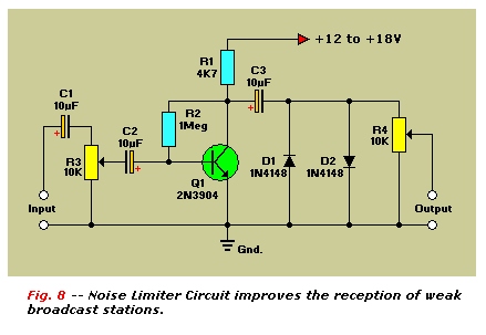
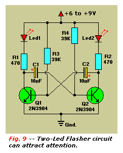
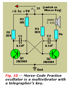
Figure 10 is a simple variation of the Fig. 9 astable multivibrator. This circuit
generates an asymmetrical waveform at about 800 Hz, which is fed to speaker SPKR1 and limiting resistor Rx in the
collector circuit of Q2. A monotone audio signal is generated when switch S1 is closed.
This circuit becomes a simple sound generator if S1 is a simple on-off switch, or it can be a Morse-code practice
oscillator if a telegrapher's key is substituted for S1. The frequency of the generated tone can be changed by altering
the values of either or both capacitors C1 and C2.
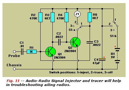 Figure 11 shows how an astable multivibrator can act as a signal injector-tracer for
testing radio receivers. When S1 is in the inject position 1, transistors Q1 and Q2 are configured as a 1KHz
astable multivibrator. With that setting, a sharp squarewave signal is sent to the probe terminal through R1
and C1.
Figure 11 shows how an astable multivibrator can act as a signal injector-tracer for
testing radio receivers. When S1 is in the inject position 1, transistors Q1 and Q2 are configured as a 1KHz
astable multivibrator. With that setting, a sharp squarewave signal is sent to the probe terminal through R1
and C1.
That waveform, which is rich in harmonics, will produce an audible output through a radio's loudspeaker if it is
injected into any audio- or radio-frequency stage of an amplitude modulated radio. By selecting a suitable injection
point, the injector can help in troubleshooting a defective radio.
When S1 is switched to Trace position 2, the circuit is configured as a cascaded pair of common-emitter
amplifiers. The Probe input feeds the base of Q1 and Q2's output driving headphone Z1. Consequently, any
weak audio signal fed to the Probe will be amplified directly and heard in the headphone.
Similarly, any amplitude-modulated radio-frequency signals that are fed to the Probe will be demodulated by the
non-linear response of transistor Q1, and the resulting audio signal will be amplified and heard in the earphone. If
the Probe is connected at suitable test points in a radio, the tracer can troubleshoot faults.
 LC Oscillators:
Many applications can be found for inductance-capacitance (L/C) oscillators in test equipment and practical circuits.
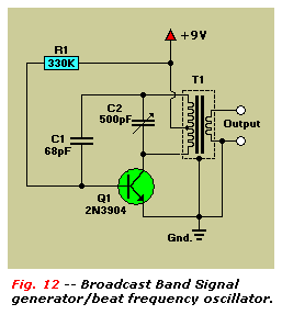
Figure 12 is a local oscillator Beat-Frequency Oscillator (BFO). Transistor Q1 is
configured as a conventional Hartley Oscillator with modified 465 KHz Intermediate Frequency (IF) transformer as its
collector load.
If the internal tuning capacitor of the transformer is removed, variable capacitor C1 becomes the tuning control of a
variable-frequency oscillator. The output frequency can be varied from well below 465 KHz to well above 1.7MHz.
Any radio capable of receiving broadcast band frequencies will detect the oscillation frequency if it is placed near
the signal generator circuit. If the signal generator is tuned to the intermediate frequency of a radio, a beat note
can be heard. This will permit continuous-wave or sinus-sideband transmissions to be detected.
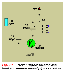
Figure 13 is a modification of Fig. 12 without a transformer secondary. When the circuit
is functioning with a nearby radio receiver acting as a detector and amplifier, it becomes a simple metal object
locator. Oscillator coil L1 is made by winding 30 turns of wire tightly on a 3- to 4-inch diameter plastic core or
bobbin about 1 inch long. It becomes a search head or sensing coil when it it is connected to the
circuit with a 3-wire cable.
 The searching head or sensor can be mounted at the end of a long wooden or plastic handle if you want to use the
circuit as a classic ground-sweeping metal detector. Similar circuits can detect buried treasure of military mines
that include at least some metal parts. However, the complete circuit can be housed in a handheld case if you want to
locate metal pipes or wiring that are hidden behind walls that are made of brick, wood, or plasterboard (gypsum/drywall).
The searching head or sensor can be mounted at the end of a long wooden or plastic handle if you want to use the
circuit as a classic ground-sweeping metal detector. Similar circuits can detect buried treasure of military mines
that include at least some metal parts. However, the complete circuit can be housed in a handheld case if you want to
locate metal pipes or wiring that are hidden behind walls that are made of brick, wood, or plasterboard (gypsum/drywall).
The operation of the object locator circuit in Fig. 13 depends on the presence of a metal
object that will interfere with coil L1's electromagnetic field. The presence of the metal object can be detected by
a battery-portable broadcast band radio held close to the locator circuit. It senses the frequency shift and gives
out an audible screech.
To detect a hidden metal object, first tune the radio to a local station, and then adjust C1 so that a low-frequency
beat or chirp is heard from the radio's speaker. This beat note will change significantly if the locator
circuit is placed near the hidden metal object.
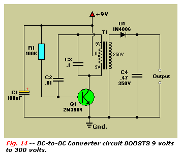
Figure 14 shows the Hartley oscillator used as a DC-to-DC converter. It is capable of
converting the output of a 9-volt battery to 300-volts DC. TransformerT1 is a 9-0-9 to 250-volt transformer. Its
primary forms the inductance (L) part of the oscillator.
 The supply voltage is stepped up to a peak of about 350 volts at T1's secondary. This waveform is rectified by
half-wave rectifier diode D1, and it charges capacitor C4. With a permanent load, the output falls to about 300 volts
at a load current of a few milliamperes.
The supply voltage is stepped up to a peak of about 350 volts at T1's secondary. This waveform is rectified by
half-wave rectifier diode D1, and it charges capacitor C4. With a permanent load, the output falls to about 300 volts
at a load current of a few milliamperes.
Caution: Without a permanent load across C4, the capacitor can deliver a powerful but non-lethal shock
to the unwary!
Conductive Water Switch:
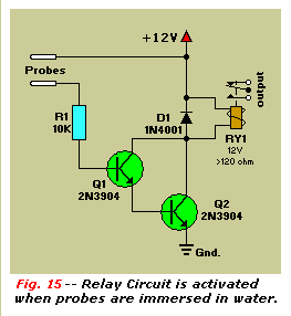
A relay switch in a circuit that can be activated when a pair of probes come in contact with water can be very useful
around the home or on a boat. It might, for example, indicate flooding of a basement, or water in the bilges of a
boat. Figure 15 is a conductive-water-operated relay. Transistors Q1 and Q2 are a
Darlington pair configured as a common-emitter, and relay coil RY1 is the collector load.
The circuit relay is normally open (NO), but it is activated when the probes are placed across a resistance path that
has a value generally less than several megohms. Most potable tap water has a bulk resistances below this value, so
this circuit will work as a water-level relay switch. Relay RY1 can activate a pump or alarm (or both). However, the
presence of salt in theater (or sea water) has higher conductivity, and it can enhance the effectiveness of the
detection circuit.
Because the conductivity of human shin has about the same resistance range as ordinary tap water, placing the probes in
contact with human skin can also serve to activate the relay.
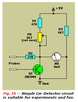 Lie Detector:
Figure 16 is simple Wheatstone bridge "lie-detector". However, because of the possible
errors in the output of this circuit, its use should be confined to games or informal experiment. The circuit's
operation is based on the knowledge that the resistance of human skin changes as a result of changes in the emotional
state of the subject.
The bridge of this detector circuit is formed by resistor R1 and R3 in a second arm. T4 in a third arm, and transistor
a probe in its base circuit) in the fourth arm.
A milliammeter with its zero point at the cent of the scale is connected across the bridge. It serves as a bridge-imbalance detector. Resistor R2 in series with the second probe is attached to the junction between Q1's collector and the low side of potentiometer R5. Large bare copper bards or silver spoons can be used to make suitable probes.
The probes should be taped or strapped directly to the skin on the subject's hand or arm, separated by at least several inches. When the subject is relaxed and his or her skin resistance reaches a stable value, adjust potentiometer R5 to obtain a null on milliammeter M1. The subject can then be questioned about the truth or falsity of emotionally loaded or embarrassing subject--in fun of course.
The subject's skin resistance will change in response to questions of that kind if they are phrased correctly. The bridge should be unbalanced if the subject reacts emotionally to the questions. Experiments of this kind are often performed by students taking college-level experimental psychology lab courses, but the equipment that they use is usually more sophisticated and sensitive than this circuit.
Professional lie detectors typically factor in changes in the subject's respiration and pulse rate measured by other sensors to supplement the skin-resistance changes. The output of the machine is in the form of pen traces on a moving pater strip. Nevertheless, you might be surprised with the results you get experimenting with this simple circuit.
Suggested Reading:
- "The Early History of the Transistor".
- "A History of Engineering and Science in the Bell System:", Physical Sciences (1925-1980). S. Millman, Editor.
- "Revolution in Miniature:", The History and Impact of Semiconductor electronics.
- "Crystal Fire", by Michael Riordan and Lillian Hoddeson
- "Transistorized!", Morgan Sparks interview.
- "How we Built the Transistor" by William Shockley. New Scientist December 1972.
- "The Improbable Years," Electronics (19 February 1968)
- "They Had Eight Days to Learn About Transistors"
Copyright and Credits:
© Original author Ray Marston. Published by Gernsback Publishing. (Hugo
Gernsback Publishing is (sadly) out of business since January 2000).
Re-posting or taking graphics in any way or form from this website or of this project is expressly prohibited by
international copyright © laws. Permission by written permission only.
Continue with Transistor Tutorial Part 7
Copyright © 2006 - Tony van Roon, VA3AVR
Last updated: December 18, 2009