Transistors Tutorial
Part 7:
"Oscillators"
"Learn about transistor oscillators and multivibrators that generate useful
sine and square waves."
Rewritten and modified by Tony van Roon
 Oscillators based on the bipolar junction transistor (BJT) are the subjects of this article. Previous articles in this
series have included articles on the characteristics of the bipolar junction transistor, the common-collector amplifier,
common-emitter and common-base voltage amplifiers, etc.
Oscillators based on the bipolar junction transistor (BJT) are the subjects of this article. Previous articles in this
series have included articles on the characteristics of the bipolar junction transistor, the common-collector amplifier,
common-emitter and common-base voltage amplifiers, etc.
Oscillator Fundamentals:
An oscillator is a circuit that is capable of a sustained AC output signal obtained by converting input energy.
Oscillators can be designed to generate a variety of signal waveforms, and they are convenient sources of sinusoidal
AC signals for testing, control, and frequency conversion. Oscillators can also generate square waves, ramps, or
pulses for switching, signalling, and control.
Simple oscillators produce sinewaves, but another form, the multivibrator, produces square or sawtooth waves. These
circuits were developed with vacuum-tubes, but have since been converted to transistor oscillators.
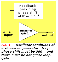
Figure 1 is a simple block diagram showing an amplifier and a block representing the
many oscillator phase-shift methods. Regardless of its amplifier, an oscillator must meet the two Barkhousen
conditions for oscillation:
1 - The loop gain must be slightly greater than unity.
2 - The loop phase shift must be 0° or 360°.
To meet these conditions the oscillator circuit must include some form of amplifier, and a portion of its output must
be fed back regeneratively to the input. In other words, the feedback voltage must be positive so it is in phase with
the original excitation voltage at the input. Moreover, the feedback must be sufficient to overcome the losses in the
input circuit (gain equal to or greater than unity).
If the gain of the amplifier is less than unity, the circuit will not oscillate, and if it is significantly greater
than unity, the circuit will be over-driven and produce distorted (non-sinusoidal) waveforms.
As you will learn, the typical amplifier--vacuum tube, BJT, or field-effect transistor--imparts a 180° phase shift
in the input signal, and the resistive-capacitive (RC) feedback loop imparts the additional 180° so that the signal
is returned in phase. Energy coupled back to the input by inductive methods can, however, be returned with zero phase
shift with respect to the input.
Specialized oscillators such as the Gunn diodes and Klystron tubes oscillate because of negative resistance effects,
but the basic oscillator principles apply here as well.
 RC Oscillators:
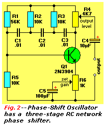
Figure 2 is the schematic for a phase-shift oscillator, a basic resistive-capacitive
oscillator. Transistor Q1 is configured as a common-emitter amplifier, and its output (collector)signal is fed back to
its input (base) through a three-stage RC ladder network, which includes R5 and C1, R2 and C2, and R3 and C3.
Each of the three RC stages in this ladder introduces a 60° phase shift between its input and output terminals so
the sum of those three phase shifts provides the overall 180° required for oscillation. The phase shift per stage
depends on both the frequency of the input signal and the values of the resistors and capacitors in the network.
The values of the three RC ladder network capacitors C1, C2, and C3 are equal as are the values of the the three
resistors R5, R2, and R3. With the component values shown in Fig. 2, the 180° phase shift occurs at about 1/14 RC
or 700 Hz. Because the transistor shifts the phase of the incoming signal 180°, the circuit also oscillates at
about 700 Hz.
 At the oscillation frequency, the three-stage ladder network has an attenuation factor of about 29. The gain of the
transistor can be adjusted with trimmer potentiometer R6 in the emitter circuit to compensate for signal loss and
provide the near unity gain required for generating stable sinewaves. To ensure stable oscillation, R6 should be set
to obtain a slightly distorted sinewave output.
At the oscillation frequency, the three-stage ladder network has an attenuation factor of about 29. The gain of the
transistor can be adjusted with trimmer potentiometer R6 in the emitter circuit to compensate for signal loss and
provide the near unity gain required for generating stable sinewaves. To ensure stable oscillation, R6 should be set
to obtain a slightly distorted sinewave output.
The amplitude of the output signal can be varied with trimmer potentiometer R4. Although this simple phase-shift
oscillator requires only a single transistor, it has several drawbacks: poor gain stability and limited tuning range.
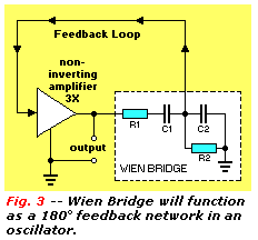
There are ways to overcome the drawbacks of the phase-shift oscillator, and one of them is to include a Wien-bridge
or network in the oscillator's feedback loop. The concept is illustrated in the Fig. 3 block diagram. A far more
versatile RC oscillator than the phase-shift oscillator, its operating frequency can be varied easily.
As shown within the dotted box in Fig. 3, a Wien Bridge consists of a series-connected resistor and capacitor, wired
to a parallel- connected resistor and capacitor. The component values are "balanced" so that R1 equals R2 and C1
equals C2.
The Wien Network is exceptionally sensitive to frequency. That shift is negative (to a maximum of -90°) at low
frequencies, and positive (to a maximum of +90°) at high frequencies. It is zero a center frequency of 1/6.28RC.
At the center frequency, network attenuation is a factor of 3.
As a result, the Wien network will oscillate if a non-inverting, amplifier with a gain of 3 is connected as shown
between the amplifier's output and input terminals. The output is taken between the output of the amplifier and
ground.
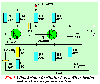
 A basic two-stage Wien-Bridge oscillator schematic is shown in Fig. 4. Both transistors
Q1 and Q2 are configured as low-gain common-emitter amplifiers. The voltage gain of Q2 is slightly greater than unity,
and it provides the 180° phase shift required for regenerative feedback. The 4.7K resistor R4, part of the Wien
bridge network, functions as the oscillator's collector load.
A basic two-stage Wien-Bridge oscillator schematic is shown in Fig. 4. Both transistors
Q1 and Q2 are configured as low-gain common-emitter amplifiers. The voltage gain of Q2 is slightly greater than unity,
and it provides the 180° phase shift required for regenerative feedback. The 4.7K resistor R4, part of the Wien
bridge network, functions as the oscillator's collector load.
Transistor Q1 provides the high input impedance for the output of the Wien network. Trimmer potentiometer R5 will set
the oscillator's gain over a limited range. With the component values shown, the Wien bridge oscillator will
oscillate at about 1 KHz. Trimmer R5 should be adjusted so that the sinewave output signal is just slightly distorted
to achieve its maximum stability.
Many different practical variable-frequency Wien-bridge oscillators can be built with operational amplifier integrated
circuits combined with an automatic gain-control feedback network. No inductors are needed in these circuits.
LC Oscillators:
Resistive-capacitive sine wave oscillators can generate signals from a few hertz up to several megahertz, but
inductive-capacitive (LC) oscillators can generate sinewave outputs from 20 or 30 KHz up to UHF frequencies.
An LC oscillator includes an LC network that provides the frequency-selective feedback between the output of the
amplifier and its input terminals.
Because of the inherently high Q or frequency selectivity of LC networks or resonant tank circuits, LC
oscillators produce more precise sinewave outputs--even when the loop gain of the circuit is far greater than unity.
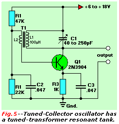
 The tuned-collector oscillator shown in Fig. 5 is the simplest of many different
LC oscillators. Transistor Q1 is configured as a common-emitter amplifier, with its base bias provided by the junction
of series resistors R1 and R2. Emitter resistor R3 is decoupled from high-frequency signals by capacitor C3.
The tuned-collector oscillator shown in Fig. 5 is the simplest of many different
LC oscillators. Transistor Q1 is configured as a common-emitter amplifier, with its base bias provided by the junction
of series resistors R1 and R2. Emitter resistor R3 is decoupled from high-frequency signals by capacitor C3.
The primary turns of transformer T1 (L1) in parallel with trimmer capacitor C1 form a tuned collector resonant tank
circuit. Collector-to-base feedback is provided by coil L2 in transformer T1. Coil L2, with a smaller number of turns
than L1, is inductively couple to L1 by transformer action.
The necessary zero phase shift around the feedback loop can be obtained by adjusting trimmer capacitor C1. If loop
gain exceeds unity at the tuned frequency, the circuit will oscillate. Loop gain is determined by the turns ratio of
L1 with respect to L2 in transformer T1.
The phase relationship between the energizing current of all LC tuned circuits and inducted voltage varies over the
range of -90° to +90°, and it is zero at a center frequency given by the formula:
 .
.
Because the circuit in Fig. 5 provides a 0° overall phase shift, it oscillates at this center frequency. The
frequency can be varied by trimmer capacitor C1 from 1MHz to 2 MHz. The circuit can be enhanced to oscillate at
frequencies from less than 100 Hz to UHF (Ultra High Frequency) frequencies with a laminated iron-core transformer.
The same circuit will oscillate satisfactorily in the UHF regions with an air-core transformer.
 Classic LC Oscillators:
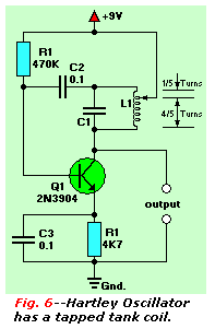
Figure 6 illustrates the Hartley Oscillator, which is a variation of the tuned-collector
oscillator that was shown in Fig. 5. This oscillator is recognizable by the tapped coil in its tuned resonant circuit.
Oscillation of the Hartley oscillator circuit depends on phase-splitting autotransformer action of the tapped coil in
the tuned resonant circuit.
The tap is located on load inductor L1 about 20% of the way down from its top so that about 1/5 of the turns are above
the tap and 4/5 are below. The positive power supply is connected to the tap to obtain the necessary
autotransformer action.
The signal voltage across the top of L1 is 180° out-of-phase with he signal voltage across its lower end, which
is connected to the collector of Q1. The signal from the top of the coil is coupled to the base (input) of Q1 through
isolating capacitor C2. The oscillator will oscillate at a center frequency determined by its LC product.
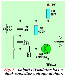
The Colpitts Oscillator shown in Fig. 7 is another classic circuit. It is
identified by the voltage divider in its tuned resonant circuit. With the component values shown, this Colpitts
circuit will oscillate at about 37KHz.
Capacitor C1 is in parallel with the output capacitance of Q1, and C2 is in parallel with the input capacitance of Q1.
Consequently, changes in Q1's capacitance (due to temperature changes or aging) can shift the oscillator frequency.
This shift can be minimized for high frequency stability by selecting values of C1 and C2 that are relative to the
internal capacitances of Q1.
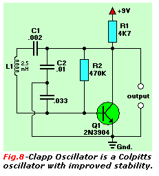
The Clapp Oscillator, a modification of the Colpitts oscillator, shown in Fig. 8,
offers higher frequency stability than the Colpitts oscillator.
This is achieved by adding capacitor C1 in series with the
coil in the tuned resonant tank circuit. It is selected to have a value that is small with respect to C2 and C3.
As a result of the presence of this capacitor, the resonant frequency of the tank and oscillator will be determined
primarily by the values of L1 and C1.
Capacitor C3 essentially eliminates transistor capacitance variations as a factor in determining the Clapp oscillator's
resonant frequency. With the component values shown, the Clapp oscillator oscillates at about 80KHz.
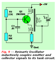
Figure 9 shows the classic Reinartz Oscillator. In this circuit, tuning coil L1
in the collector circuit and the tuning coil L2 in the emitter circuit are inductively coupled to tuning coil L3 in
the resonant tank circuit. Positive feedback is obtained by coupling the collector and emitter signals of the
transistor through windings L1 and L2, and inductively coupling both of these coils to L3. This Reinartz oscillator
oscillates at a frequency determined by L3 and trimmer capacitor C2. With the values and turns ratios given in
Fig. 9, the circuit will oscillate at a few hundred KHz.
 Modulation:
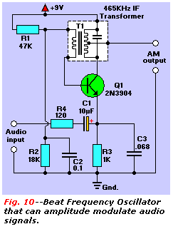
The LC oscillator circuits shown in Figs. 5 to 9 can be modified to produce amplitude- or frequency-modulated (AM or
FM) rather than continuous wave (CW) output signals. Figure 10 is the schematic for a
beat-frequency oscillator (BFO). It is based on the tuned-collector circuit of Fig. 5, but modified to become a
465-KHz amplitude-modulated (AM) BFO.
A standard 465-KHz IF transformer (T1), intended for transistor circuits, is the LC resonant tank circuit in this
oscillator. An audio-frequency AM signal fed to the emitter of Q1 through blocking capacitor C2 will modulate the
supply voltage of Q1 and thus amplitude-modulate the circuit's 465-KHz carrier signal.
This BFO can provide 40% signal modulation. The value of emitter-decoupling capacitor C1 was selected to present a low
impedance to the 465-KHz carrier signal, while also presenting a high impedance to the low-frequency modulation signal.
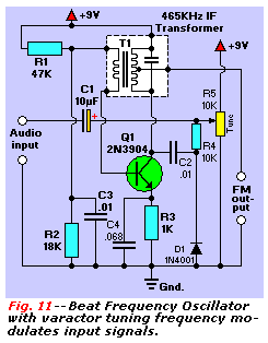
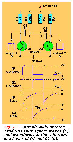 Figure 11 shows how the BFO circuit in Fig. 10 can be modified to become a frequency
modulator. Tuning is adjusted by trimmer potentiometer R5. Silicon diode D1 functions as an inexpensive varactor
diode. A 1N4001 diode frequency modulates the 465-KHz BFO circuit. Here, C2 and diode "capacitor" D1 are in series.
Figure 11 shows how the BFO circuit in Fig. 10 can be modified to become a frequency
modulator. Tuning is adjusted by trimmer potentiometer R5. Silicon diode D1 functions as an inexpensive varactor
diode. A 1N4001 diode frequency modulates the 465-KHz BFO circuit. Here, C2 and diode "capacitor" D1 are in series.
Consequently, the oscillator's center frequency cam be changed by altering the capacitance of D1 with trimmer
potentiometer R5, and frequency-modulated signals can be obtained by introducing an audio-frequency modulation signal
to D1 through C1 and R4. Capacitor C2 provides DC isolation between Q1 and D1.
Astable Oscillators:
Conventional oscillator circuits produce sinewaves, but repetitive square waves are important in electronics. One way
to generate them is with the astable multivibrator circuit shown in Fig. 12a.
This multivibrator is a self-oscillating regenerative switch whose on and off periods are controlled by the time constants
obtained as the products of R2 and C2, and R3 and C1. If these time constants are equal (because both values of R
and C are equal), the circuit becomes a square-wave generator that operates at a frequency of about 1/1.4 RC. The
waveforms taken at the collector and base of transistors Q1 and Q2 are shown in
Fig. 12b.
The frequency of the astable multivibrator in Fig. 12 can be decreased by increasing the values of C1 and C2 or R2 and
R3, or increased by decreasing them. The frequency can be varied with dual-gang variable resistors placed in series
with 10K limiting resistors in place of R2 and R3.
The operating frequency can, if required, be synchronized to that of a higher-frequency signal by coupling part of the
external signal into the timing networks of the astable circuit. Outputs can be taken from either collector of the
circuit, and the two outputs are in opposite in phase. The multivibrator's operating frequency is essentially
independent of power supply voltage between + 1.5 and + 9 volts.
The upper voltage limit is set by inherent transistor behavior: as the transistors change state at the end of each
half-cycle, the base-emitter junction of one transistor is reverse biased by a voltage that is about equal to the supply
voltage. Consequently, if the supply voltage exceeds the reverse base-emitter breakdown voltage of the transistor,
circuit timing will be affected.
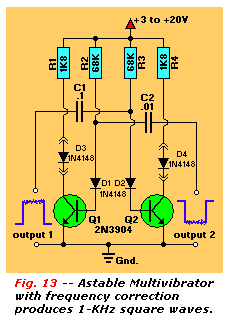 This characteristic can be overcome with the circuitry modifications shown in Fig. 13.
A silicon diode is connected in series with the base input terminal of each transistor to raise the effective
base-emitter reverse breakdown voltage of each transistor to a value greater than that of the diode.
This characteristic can be overcome with the circuitry modifications shown in Fig. 13.
A silicon diode is connected in series with the base input terminal of each transistor to raise the effective
base-emitter reverse breakdown voltage of each transistor to a value greater than that of the diode.
The protected astable multivibrator will operate with any supply voltage from +3 to +20 volts. Its frequency will vary
only about 2% when the supply voltage is varied from +6 to +18 volts. This variation can be further reduced to 0.5% by
adding another "compensation" diode in series with the collector of each transistor, as shown in Fig. 13.
Multivibrator Variations:
The basic astable multivibrator shown in Fig. 12 can be modified in different ways to improve its performance or
change the shape of its output waveform. Some modifications are shown in Figs. 14 to 18.
A shortcoming of the multivibrator shown in Fig. 12 is that the leading edge of each of its output waveforms is
slightly rounded. The lower the values of timing resistors R2 and R3 with respect to collector load resistors R1 and
R4, the more pronounced will be this waveform rounding.
Conversely, the larger the values of R2 and R3 with respect to R1 and R4, the sharper the waveform edge will be. The
maximum permissible values of R1 and R4 are, however, limited by the current gains of the transistors. These gains are
equal to hFE multiplied wither by the value of resistor R1 or R4.
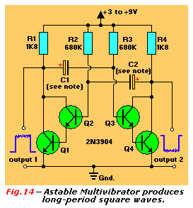
 One way to improve the circuit waveform, of course, would be to replace transistors Q1 and Q2 with Darlington
transistor pairs and then substitute timing resistance values that are as large as permissible. That is done in the
long-period astable multivibrator that is shown in Fig. 14.
One way to improve the circuit waveform, of course, would be to replace transistors Q1 and Q2 with Darlington
transistor pairs and then substitute timing resistance values that are as large as permissible. That is done in the
long-period astable multivibrator that is shown in Fig. 14.
Resistors R2 and R3 can have any value between 10K and 12Meg, and the multivibrator will run from any supply voltage
between +3 and +18 volts. With R2 and R3 values shown in Fig. 14, the multivibrator's total period or cycle time is
about 1 second per microfarad when C1 and C2 have equal values. This multivibrator generates sharp-cornered square
waves.
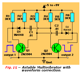
The square waves with the rounded leading edges produced by the multivibrator shown in Fig. 12 are caused by an
inherent characteristic of the transistor. As each transistor is switched off, its collector voltage is prevented
from switching abruptly to the positive supply value. This is due to the loading between that collector and the base
of the adjacent conducting transistor from timing capacitor cross-coupling.
 This characteristic can be altered, and sharp square waves can be obtained by effectively disconnecting the timing
capacitor from the collector of its transistor as it turns off. That improvement is shown in
Fig. 15, a schematic for a 1-KHz astable multivibrator. It includes diodes D1 and D2 that
disconnect the timing capacitors at the moment of switching.
This characteristic can be altered, and sharp square waves can be obtained by effectively disconnecting the timing
capacitor from the collector of its transistor as it turns off. That improvement is shown in
Fig. 15, a schematic for a 1-KHz astable multivibrator. It includes diodes D1 and D2 that
disconnect the timing capacitors at the moment of switching.
The important time constants of the multivibrator in Fig. 15 are also determined by C1 and R4, and C2 and R1. The
effective collector loads of Q1 and Q2 are equal to the parallel resistances of R1 and R2, and R5 and R6, respectively.
Basic astable multivibrator operation depends on slight differences in their transistor characteristics. Those
differences cause one transistor to turn on faster than the other when power is first applied, thus triggering
oscillation.
If the multivibrator's supply voltage is applied slowly by increasing it from zero, however, both transistors could turn
on simultaneously. If this happens, the oscillator will be a nonstarter.
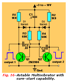
The possibility of nonstarting can be avoided with the "sure-start" astable multivibrator circuit shown in
Fig. 16. There, the timing resistors are connected to the transistor's collectors so that
only one transistor can conduct at a time, ensuring that oscillation will always begin.
 All the astable multivibrator circuits shown so far are intended to produce symmetrical output waveforms, with a 1 to 1
ratio of square wave to space (1:1 mark/space ratio). Non-symmetrical waveforms can be obtained by installing one set
of RC astable time constant components that is larger than the other.
All the astable multivibrator circuits shown so far are intended to produce symmetrical output waveforms, with a 1 to 1
ratio of square wave to space (1:1 mark/space ratio). Non-symmetrical waveforms can be obtained by installing one set
of RC astable time constant components that is larger than the other.
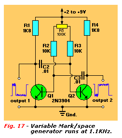
Figure 17 shows a 1.1KHz variable mark/space ratio generator. The ratio can be varied
over the range 1 to 10 with trimmer potentiometer R5. However, the leading edges of the output waveforms of this
circuit could be too round for some applications when mark/space control is set at its extreme position. Also, this
generator could be difficult to start if the supply voltage is applied slowly to the circuit.
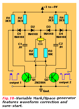
Both of the drawbacks can be overcome with the modifications shown in the schematic of Fig. 18,
another 1.1KHz variable mark/space ratio generator. The circuit includes both sure-start and waveform-correction
diodes.
Copyright and Credits:
© 1993 Original author Ray Marston. Electronics Now, December 1993. Published by
Gernsback Publishing. (Hugo Gernsback Publishing is (sadly) out of business since January 2000).
All graphics, drawings, photos, © 2006 Tony van Roon.
Re-posting or taking graphics in any way or form from this website or of this project is expressly prohibited by
international copyright laws. Permission by written consent only.
Continue with Transistor Tutorial Part 8
Copyright © 2006 - Tony van Roon, VA3AVR
Last updated: December 18, 2009