Transistors Tutorial
Part 8:
"Amplifier Design"
"It's easy to design a simple transistor amplifier. Here is how."
Rewritten & modified by Tony van Roon
We were having trouble finding an exact replacement transistor while repairing a piece of equipment. Figuring that an
exact replacement was going to be impossible to find, we began to discuss what to do. And someone pointed out that
there were only two kinds of bipolar transistors--NPN and PNP. Of course, values for various characteristics vary
widely, even for a specific transistor; but in many circuits, a garden-variety device will work (and did in our case).
Designing and repairing transistorized circuits is much simple than you might suspect. A well-designed circuit has
built-in tolerance, so it's probably not device sensitive. The most important characteristics to consider when
substituting devices or designing a circuit from scratch are operating frequency and power level.
What follows is the design procedure we went through to solve an audio-gain problem. Try it when you need a little
extra gain for that next audio project.
An Audio Amp:
This particular project involved injecting the audio from a TV receiver into a stereo system. (These days even the
cheapest TV has that feature, including MTS stereo inputs for digital accessories). Anyways, the audio-output portion
of the TV-audio receiver was abandoned because of its poor frequency response and high distortion. Instead, we wanted
to come right off the detector into a quality audio amplifier and speaker. So, after picking off the audio at a
convenient point in the set (in this case, from a potentiometer), we wanted to feed it to the auxiliary input of the
stereo amplifier.
The amplifier we used required an input of 1 volt RMS, but a quick check with an AC VTVM indicated that out picked-off
audio signal was only 0.1-volt RMS. Obviously, an amplifier with a gain of 10 was needed.
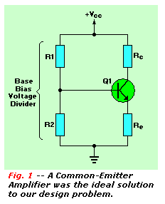
Scanning the literature on transistor amplifiers reveled that a common-emitter amplifier with a voltage-divider bias
circuit would solve our problem nicely. Such a circuit is shown in Fig. 1. Some of that
circuit's characteristics include: moderate input impedance, moderate voltage gain, inverted output, and input/output
impedance and gain that depend only slight on transistor beta.
There are, of course, several rules that must be followed in using a common-emitter amplifier, including:
- With a positive supply use an NPN transistor.
- With a negative supply use an PNP transistor.
- The supply voltage must not exceed the transistor's Vce rating.
- The power-dissipation rating of the transistor must not be exceeded.
- The beta of the transistor should be 100 or higher.
 In our example the following facts are known:
- Our amplifier had a single-ended 12-volt power supply.
- We need a voltage gain of 100.
- The input impedance of the amplifier should be about 15K, the same as the potentiometer from which the audio was
taken.
- The impedance of the stereo amplifier's auxiliary input is about 50K.
As is the case in most circuit designs, a few facts are known, and the rest must be calculated or picked using a a few
"rules of thumb". We will learn how to make the calculations next.
Doing the Math:
For maximum undistorted output swing, we will make the quiescent collector voltage 1/2 the supply voltage. See
Fig. 2. The drop across Rc must therefore be 6 volts.
The value of Rc, the collector load resistance, is chosen considering output impedance, gain, and collector current.
If possible, the output impedance should be lower than the impedance of the circuit we are feeding by a factor of 10
or more. Doing so will avoid circuit loading. So let's make Rc equal to 4700 ohms, which is about 50K/10.
Collector current Ic, is equal to 0.5Vcc/Rc, or 6/4700 = 1.28 mA. That current is
certainly low enough that we will not exceed any collector-current ratings, so let's go on.
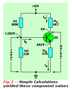 To achieve maximum stability, the emitter resistor should be in the range of 40 to 1000 ohms. Voltage gain
(Av) = Rc/Re, so Re = Rc/Av. In our case
Re equals 4700/10, or 470 ohms. That falls within the range of acceptable values.
To achieve maximum stability, the emitter resistor should be in the range of 40 to 1000 ohms. Voltage gain
(Av) = Rc/Re, so Re = Rc/Av. In our case
Re equals 4700/10, or 470 ohms. That falls within the range of acceptable values.
The current through the emitter resistor consists of the collector current plus the base current. The base current
here is significantly smaller than the collector current, so it can be ignored for the next calculation.
The voltage drop across the emitter resistor = Ic X Re, or 1.28 mA x 470 ohms = 0.602 volts.
The base voltage must exceed the emitter voltage by 0.6 volts for a silicon transistor and by 0.2 volts for a germanium
transistor. We'll use a silicon transistor (most if not all germanium types are obsolete) in our circuit, so the base
voltage must be 0.6 + 0.602 = 1.202 volts.
The input impedance of the circuit equals R2 in parallel with the emitter resistor times beta; input impedance will
vary with the transistor's beta. FOr our example, assume we are using a transistor with a beta of 100. We want the
input impedance to be about 15000 ohms. Solving for R2, we find:
    Zin = (R2 X Re X beta)/[R2 + (Re X beta)]
    R2 = (Zin X Re X beta)[(Re X beta) - Zin]
    R2 = (15000 x 470 x 100)/[470 x 100) - 15000]
    R2 = 22,030 ohms.
We can use a 22K resistor. In general, if input impedance is not critical, for maximum stability R2 can be 10 to 20
times Re.
The drop across R2 must be 1.20 volts so the current through R2 is 1.20/22,000, or 0.054 mA. Therefore, R1 must drop
the rest of the supply voltage, which is 12 - 1.20 = 10.8 volts. The current flowing through R1 is a combination of
the voltage-divider current plus the base current.
The base current is equal to the collector current divided by beta. It is found from:
Ibeta = 1.28/100 = 0.0128 mA
So the total current through R1 is 0.054mA + 0.0128mA = 0.067mA, and R1 = 10.8/0.067mA = 160,000 ohms (160K).
 Resistor R1 is the most critical resistor in the circuit. To ensure maximum voltage swing, it should bring the
quiescent collector voltage to one half the supply voltage. After building the circuit, the value of R1 may have to
be varied slightly to achieve that voltage swing.
Resistor R1 is the most critical resistor in the circuit. To ensure maximum voltage swing, it should bring the
quiescent collector voltage to one half the supply voltage. After building the circuit, the value of R1 may have to
be varied slightly to achieve that voltage swing.
We now have a circuit we can test.
Interfacing:
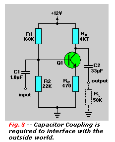
Connecting the circuit to the outside world will require capacitor coupling. That serves to isolate the AC signal
from any DC bias voltages. Figure 3 shows our complete circuit with input and output
coupling capacitors. The values of those capacitors were calculated using C = 1/(3.2 x ƒ x R), where C equals
the capacitor value in farads, ƒ equals the frequency at which response will be down 1dB, and R equals the
impedance on the load side of the capacitor.
To calculate the value of C1, the amplifier's input impedance (15K) is used for R. To calculate the value of C2,
the input impedance of the next stage (50K) is used for R.
The value of C1 can now be calculated for a drop of 1dB at 20 Hz: C1 = 1/(3.2 x 20 x 15000) = .00000104 farad = 1.0 uF.
The value of C2 = 1/(3.2 x 20 x 50000) = .00000031 farad = 0.33uF.
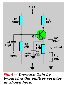
To increase the gain of the stage, you could bypass Re with a capacitor, as shown in Fig. 4.
Nothing comes for free, however. The price you pay for increase gain is lower input impedance, which will vary widely
with beta. If that variation is not a problem, a significant gain increase can be realized by adding the bypass
capacitor. Our original circuit has a gain of 10; if the emitter is bypassed the gain becomes
Rc/003/Ie = 4700/(0.03/0.00129) = 4700/23 = 200 (approx).
The value of the bypass capacitor in farads is calculated from the formula C = 1/(6.2 x ƒ x R). Again ƒ is
the low-frequency limit in Hz, and R is the dynamic emitter resistance (0.031/Ie). In our example, if we
stick to a 20-Hz lower limit we have C = 1/[6.2 x 20 x (0.03/0.00129)] = .000344 farads = 344 uF. A 350uF unit can be
used.
Thoughts:
A few thoughts on components before we finish: using 5% resistors allows closer adherence to the calculated values.
Because of their temperature stability and low leakage specifications, silicon rather than germanium transistors are
preferable for this type of circuit.
Finally, you've no doubt noticed that we have yet to specify a specific transistor. That's because for this type of
application it really doesn't matter! Almost any small signal device will do fine.
Copyright and Credits:
Copyright © of the original article by author Jack Cunkelman, published in
Radio Electronics Magazine, August 1987.
Published by Gernsback Publishing. (Hugo Gernsback Publishing is (sadly) out of business since January 2000).
Re-posting or taking graphics in any way or form from this website or of this project is expressly prohibited by
international copyright © laws. Permission by written request only.
Continue with Transistor Tutorial Part 9, FET's
Copyright © 2006 - Tony van Roon, VA3AVR
Last updated: December 18, 2009