Home » Circuits
Surf Simulator Circuit Diagram
Do you long for a beach holiday on a tropical island, but you don’t have the necessary wherewithal? We’ve got just the answer: build the i-TRIXX surf simulator, put on your headphones, and dream yourself away from this dreary realm. Let the rhythmic rush of the waves transport you to a sun-drenched beach with gently swaying palm trees, and relax for a while before returning to a chilly confrontation with reality. That’s the ultimate in low-budget travel.Book now! Isn’t it great to relax on the snow-white sand of a tropical beach with a cool drink in your hand? To enjoy the magnifi cent of earthly creation while letting your thoughts drift on the hypnotic mantra of the breaking surf? No relaxant brewed by human hands can possibly compete with it! But when you start thinking about how much it all costs, you’ll reach for the headache pills instead. Fortunately, there’s a less expensive way to relax — with a bit of electronics that imitates the soothing sound of the sea.
You’ll have to imagine the corresponding surroundings on your own. A sunlamp and a few scoops of sand may help…This circuit uses more components that most of the i-TRIXX do it yourself projects, but this doesn’t make it harder to understand how it works. We have also designed a PCB layout for the circuit, which makes DIY construction that much easier. Noise is usually the last thing you want in any sort of audio circuitry. Noise is generated in semiconductor devices (transistors and diodes) as an undesirable by-product.
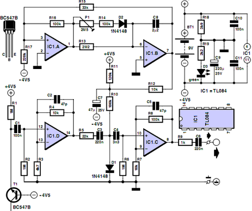
Circuit diagram:
However, in our surf simulator we just can’t get enough of it! Noise forms the basis for imitating the sound of breaking surf. We take advantage of the fact that a reverse-biased base–emitter junction of a transistor generates noise like the devil if the voltage is high enough. The noise source in the schematic diagram is transistor T1. The base–emitter junction of this transistor breaks down at approximately 7 V (depending on the specific transistor). R1 limits the current to a level that avoids destroying the transistor.
T1 generates a constant noise signal, which doesn’t resemble the sound of breaking surf. If you listen carefully to the sound of real surf, you’ll notice that it resembles a noise signal that increases rapidly in volume (as the wave rolls up the beach) and then slowly dies down. This means the noise must rise and decay in a sawtooth waveform. To achieve this effect, we make use of the AC impedance of a normal diode (D1 in the schematic diagram), which depends on the amount of DC current fl owing through the diode. The higher the current through the diode, the lower its AC impedance (and thus its impedance to the noise signal).
The voltage across R10 determines how much current flows through diode D1. The noise signal is amplified by IC1d and applied to the diode, and the voltage across the diode is further amplified by IC1c to the output level. As already mentioned, the amplitude of the noise signal depends on the DC current through diode D1. What we have to do now is make the current through D1 (or in other words, the voltage across R10) vary in a sawtooth pattern. This job is handled by amplifiers IC1a and IC1b.
You can use P1 to adjust the form of the sawtooth (and thus how the noise grows and decays) according to your taste. The circuit works best with a clean 9-V supply voltage, so an AC mains adapter with a stabilized 9-V output is the preferred choice as a power source. A balanced supply voltage is required for proper operation of the circuit, so a virtual ground is necessary.
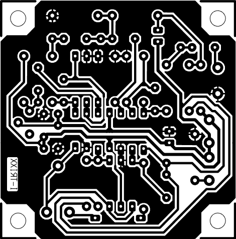
PCB layout:
Resistors
R1,R2,R6 = 1 MΩ
R3 = 4kΩ7
R4,R8,R10,R14,R16 = 100 kΩ
R5 = 22 kΩ
R7,R12 = 10 kΩ
R9 = 1 kΩ
R11 = 120 kΩ
R13 = 2MΩ2
R15 = 33 kΩ
R17 = 220 kΩ
R18 = 3kΩ9
R19 = 2kΩ2
P1 = 2MΩ5 preset
Capacitors
C1,C10,C11 = 100 nF
C2,C5 = 47 pF
C3,C6 = 220 nF
C4 = 3nF3
C7 = 47 µF/25V radial
C8 = 2µ2 MKT lead pitch 5 or 7.5mm
C9 = 220 µF/25V radial
Semiconductors
D1,D2 = 1N4148
D3 = LED, 3mm, green, low current
T1 = BC547B
IC1 = TL084
Miscellaneous
6 PCB solder pins
BT1 = 9V battery with clip-on leads
(however 9 V battery eliminator
preferred)
This is created in a simple manner by a voltage divider (R18 and R19). To reduce the current consumption (in case you want to power the circuit from a battery), it also provides a ‘power on’ indication. The current consumption of the circuit is approximately 9 mA, which means the battery would have to be replaced already after two days of continuous use if it is powered by a battery, so using an AC mains adapter is certainly advisable. We designed a PCB layout for this project to make it easier to assemble, since it is a bit more complex than most of the i-TRIXX circuits.
If you follow the illustrated component layout, you shouldn’t have any trouble at all. The idea here is that you print the copper layout at actual size (52 × 52 mm) on transparent film. The easiest way to do this is to use the supplied pdf fi le which you can open with Adobe Reader. You can then use the fi lm to expose a circuit board, develop it, and then etch it. Alternatively, you can take the fi lm to your local electronics shop and have them make a board for you.
Source: Elektor Electronics 12-2006


