Home » Circuits
Switchable Output Crystal Oscillator
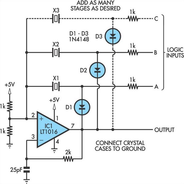
This oscillator circuit permits crystals to be electronically switched by logic commands. The circuit is best understood by initially ignoring all crystals. Furthermore, assume that all diodes are shorts and their associated 1kO resistors open. The two 1kO resistors at the non-inverting input of IC1 (LT1016) set the output to half the supply, ie, +2.5V. The RC network from the output to pin 3 sets up phase-shifted feedback and the circuit looks like a wide-band unity gain follower at DC. When crystal X1 is inserted (remember, D1 is temporarily shorted) positive feedback occurs and oscillation commences at the crystal’s resonant frequency.Circuit diagram:
If D1 and its 1kO resistor are then considered to be part of the circuit, oscillation can only continue if logic input A is biased high. Similarly, the circuit can only operate at crystal X2’s frequency if logic input B is high. Additional crystal/diode/1kO resistor branches permit logic selection of the crystal frequency. For AT cut crystals about a millisecond is required for the circuit output to stabilise due to the high Q factors involved. Crystal frequencies can be as high as 16MHz before propagation delays in the comparator prevent reliable operation.

