Home » Circuits
Frequency Doubler
If you are working at frequencies of the order of 850MHz to 4GHz and find that a frequency multiplier is required, the HMC 187, HMC 188 and HMC 189 (see table) frequency doubler may be just the solution you are looking for. The isolation performance of these devices ensures that the input frequency (fin) and its harmonics 3fin and 4fin are attenuated by 35dB relative to the wanted output frequency 2fin. This excellent isolation specification reduces the need for additional output filtering and is also an advantage where several doublers are connected in series to produce four or eight times the input frequency.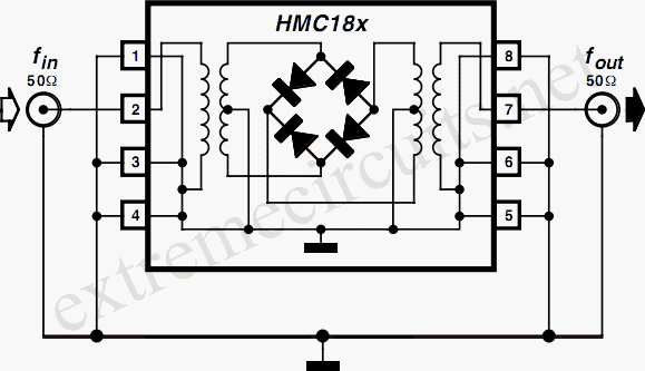 The tiny outline of the HMC18x- series device occupies a board area of 3mm by 4.8mm and measures just 1.07 mm high. Internally the device contains balanced to unbalanced transformers (baluns) to match the doubler circuit with the output and input. The doubler circuit itself is passive and comprises a full wave Schottky diode bridge rectifier. The monolithic baluns which are integrated on-chip give the device a relatively high low-frequency roll-off at 850MHz.
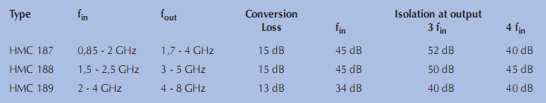 Lower frequencies can also be multiplied but the conversion loss factor (given as typically 15 dB) will increase. The input and output are matched for 50 Ohm operation and the input signal level should be of the order of +15dBm which will give a output level of approximately 0dBm. The main characteristics of the three versions of this device are summarized in the table above.