Home » Circuits
Fully Adjustable Power Supply
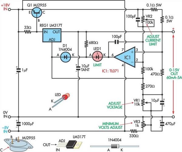
Based on a National Semiconductor application note, this circuit uses an LM317 3-terminal regulator (REG1), chosen because of its built-in over-current and over-temperature protection. Its output is boosted up to just over 5A by the MJ2955 transistor (Q1). The output voltage is varied by adjusting the voltage on REG1’s ADJ terminal using VR1 (a 10kO potentiometer), via the 270O resistor. Adjustable current limiting is provided by op amp IC1, used as a comparator, which monitors the voltage across the 0.1O current sensing resistors. Once this voltage exceeds a level set by potentiometer VR2, then its output goes low, dragging down the adjust pin of REG1 and thus the output voltage.Circuit diagram:
LED1 illuminates when current limiting is occurring. The 10kO voltage adjust potentiometer (VR1) has one side connected to -5V instead of 0V so that the output voltage can be varied down to 0V instead of 1.2V (normal limit of an LM317). Trimpot VR3 is adjusted to set the minimum output voltage to +100mV or so. Note that because the -5V rail is used as a reference, it should be regulated using an LM7905 or similar. The LM317 3-terminal regulator and Q1 should be mounted on the same heatsink to take advantage of REG1’s thermal control.
Author: Philip Chugg - Copyright: Silicon Chip Electronics

