Home » Circuits
General Purpose Oscillator
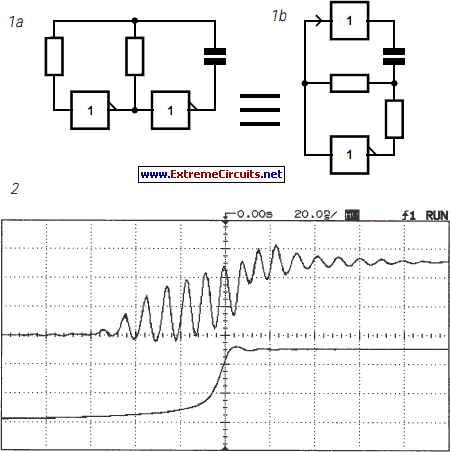
The oscillator shown in Figure1 is frequently used in digital circuits and may, therefore, look very familiar. Many readers may not know that this type of oscillator suffers from a nasty draw-back caused by noise. When the amplitude of the noise is higher than the hysteresis of the gates used for the oscillator, spurious switching pulses are generated near the zero crossings. This problem can be cured only by ensuring that the rise time of the input signal is shorter than the reaction time of the relevant gate. When the oscillator is built with fast logic gates, such as those in the HC-series, the like-lihood of the problem occurring is great.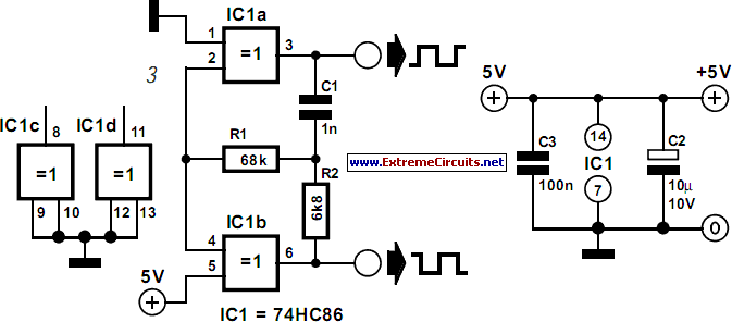 However, as long as the positive feedback is fast enough, nothing untoward will happen. However, when delays occur owing to the transit time of the components used, the problem may rear its head. In the configuration of
Figure 1a, the signal passes through two inverters and thus experiences twice the transit time of a single gate. The upper signal in the oscilloscope trace in Figure 2 shows the result of this: the gates used are simply too fast for this type of oscillator. If one of the inverters is replaced by a buffer, and the oscillator is modified as shown in Figure 1b, the transit time is limited to that of one gate: the lower trace in Figure 2 shows that the oscillator then works correctly. The practical circuit diagram of the general-purpose oscillator is shown in Figure 3. Note that two XOR gates are used to ensure that the transit time of the buffer is equal to that of the inverter.
However, as long as the positive feedback is fast enough, nothing untoward will happen. However, when delays occur owing to the transit time of the components used, the problem may rear its head. In the configuration of
Figure 1a, the signal passes through two inverters and thus experiences twice the transit time of a single gate. The upper signal in the oscilloscope trace in Figure 2 shows the result of this: the gates used are simply too fast for this type of oscillator. If one of the inverters is replaced by a buffer, and the oscillator is modified as shown in Figure 1b, the transit time is limited to that of one gate: the lower trace in Figure 2 shows that the oscillator then works correctly. The practical circuit diagram of the general-purpose oscillator is shown in Figure 3. Note that two XOR gates are used to ensure that the transit time of the buffer is equal to that of the inverter.