Home » Circuits
Oscillation Monitor
The circuit in the diagram was originally designed to monitor an oscillator, but can also be used as a general-purpose level indicator for a.c. signals. It is based on a quadruple IC containing four NAND gates. Only three of the gates are used, making the fourth free for other purposes. All the gates have a Schmitt trigger input. When a 5 V supply is used, the Type 74HC132 is recommended; for higher voltage, a Type 4093. Note, however, that these two ICs have different pinouts. In the diagram, the differing pins of a 4093 are shown in brackets. The signal to be monitored is applied to the input of the first gate via capacitor C1. Resistor R2, in conjunction with the protection diode in the IC, guards the input to high voltages.In the absence of a signal, resistor R1 holds the input high so that the output of the gate is low. When a signal of sufficient strength is received, the input of the gate goes low during the negative half cycle of the signal, so that the output of the gate goes high in rhythm with the input signal. However, the Schmitt trigger converts sinusoidal signals into rectangular ones, which charge capacitor C3 via diode D1. When the potential across C3 exceeds the threshold at the input of the second gate, this gate also toggles. The output of the second gate is then low, which disables the third gate, which functions as an oscillator. When the level of the input signal drops, C3 is discharged via R3.
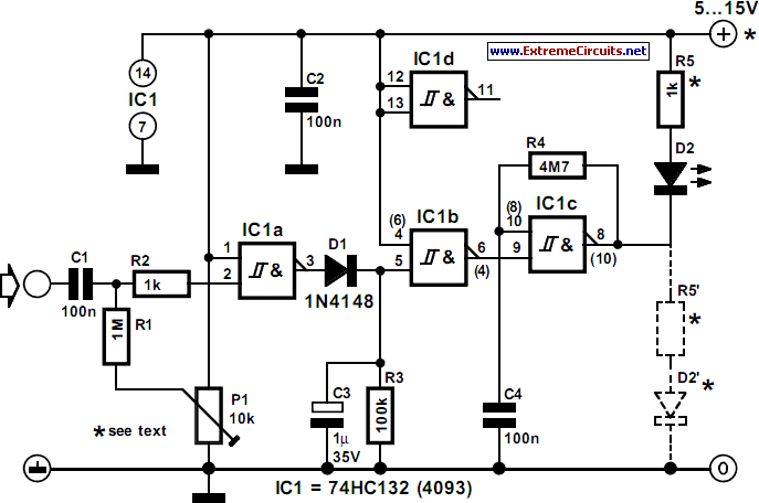
The potential across the capacitor then no longer exceeds the threshold at the input of IC1b, whereupon IC1c is enabled and the LED flashes The LED may be connected as shown or as indicated by the dashed line. As shown, the diode remains off when there is an input signal of sufficient strength and begins to flash when the signal fails or its level drops. When the diode is linked to earth, it is on continuously when there is an input signal, and begins to flash when the input drops. When a 5 V power supply is used, R5 = 1 kΩ, and the circuit draws a current, including that of the LED, of 3 mA. The frequency of the input signal may lie between 10 Hz and 10 MHz. When a 9–12 V supply is used, the value of R5 must be altered as necessary.
Owing to the 4093 being slower than the 74HC132, the upper frequency of the input signal is then limited to 3 MHz. When the wiper of P1 is at the level of the supply voltage, the response threshold, USS, lies between 3.5 V (when Ub =5V) and 7 V (when Ub =12V). When the wiper is moved away from the positive supply line, USS (max) is 1.5 V (when Ub = 5 V). The response threshold is quite precise: a drop in the input signal level of 50–100 mV is sufficient to disable the input. When the input level is too high, a preset across the input terminals enables the level to be reduced to a value that lies in the desired range above the response threshold.