Home » Circuits
Pulse Generator
This circuit is very useful while checking/operating counters, stepping relays, etc. It avoids the procedure of setting a switch for the required number of pulses. By pressing appropriate switches S1 to S9, one can get 1 to 9 negative-going clock pulses, respectively. Schmitt trigger NAND gate N1 of IC2, resistor R1, and capacitor C1 are wired to produce clock pulses. These pulses are taken out through NAND gate N3 that is controlled by decade counter CD4017 (IC1). Initially no switch from S1 to S9 is depressed and the LED is glowing. As pins 5 and 6 of NAND gate N2 are pulled up by resistor R3, its output pin 4 goes low. This disables NAND gate N3 to take its output pin 10 to high state, and no pulse is available. IC1 is a decade counter whose Q outputs normally remain low.When clock pulses are applied, its Q outputs go high successively, i.e. Q0 shifts to Q1, Q1 shifts to Q2, Q3 shifts to Q4, and so on. If any one of switches S1 through S9, say, S5 (for five pulses), is momentarily depressed, pins 5 and 6 of NAND gate N2 go low, making its output pin 4 high, which fully charges capacitor C2 via diode D. At the same time, this high output of N2 enables NAND gate N3 and clock pulses come out through pin 10. These are the required number of pulses used to check our device. The clock pulses are fed to clock-enable pin 13 of IC1, which starts counting. As soon as output pin 1 (Q5) of IC1 turns high, input pins 5 and 6 of NAND gate N2 will also become high via switch S5 because high-frequency clock allowed five pulses during momentary pressing.
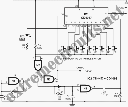 This high input of N2 provides low output at pin 4 to disable NAND gate N3 and finally no pulse will be available to advance counter IC1. Before the next usage, counter IC1 must be in the standby state, i.e. Q0 output must be in the high state. To do this, a time-delay pulse generator wired around NAND gate N4, resister R4, diode D, capacitor C2, and differentiator circuit comprising C3 and R5 is used. When output pin 4 of NAND gate N2 is low, it discharges capacitor C2 slowly through resistor R4. When the voltage across capacitor C2 goes below the lower trip point, output pin 11 of NAND gate N4 turns high and a high-going sharp pulse is produced at the junction of capacitor C3 and resistor R5.
This sharp pulse resets counter IC1 and its Q0 output (pin 3) goes high. This is represented by the glowing of LED. Ensure the red LED is glowing before proceeding to get the next pulse. Press any of the switches momentarily and the LED will glow. If the switch is kept pressed, the counter counts continuously and you cannot get the exact number of pulses.