Home » Circuits
Simple Pre-Regulator
There will be many times where it is desirable to use the P05 supply module from a higher voltage source. For example, if you want to add balanced inputs to a power amplifier, then you need a +/-15V supply, but the amp's supply voltage will be much too high for the regulator ICs.This project is about as simple as they come, and is very cheap to build. It is designed for exactly this purpose - to reduce the amplifier supply voltage to a safe value for regulator ICs.
Description:
The circuit is shown in Fig. 1 and it is very simple indeed. You will need to make a few simple calculations to determine the resistor value, but this is explained below.
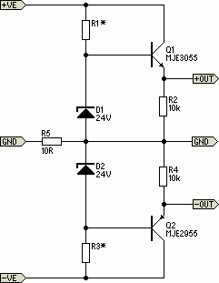 Fig. 1 Pre-Regulator Schematic
The purpose of R5 is to isolate the main power amplifier ground from the supply, to prevent hum loops. The 10Ω resistor shown will be fine for the vast majority of applications, but may need to be changed. This is up to you to experiment with if necessary. I suggest that R5 should be 1W. R2 and R4 may be 1/4W or 1/2W resistors, and 1W zeners are recommended.
The only calculation is to determine the value for R1 and R3. First, measure the power amp supply voltage (V1). The resistor value is calculated to provide a maximum zener current of 20mA, and this will ensure sufficient base current for the pass transistors for up to 100mA or so output current at ±15V.
V2 = V1 - 24 (Where V1 is amplifier supply voltage, and a 24V zener is used)
R1 = R3 = V2 / 20 (R1 and R3 values are in kΩ)
P = V2² / R1 (P is power dissipation of R1 and R3 in mW)
Let's assume a supply voltage of ±56V for an example calculation ...
V2 = 56 - 24 = 32V
R1 = R3 = 32 / 20 = 1.6k (use 1.5k)
P = 32² / 1.5 = 680mW = 0.68W (use 1W)
The dissipation in Q1 and Q2 may also be calculated, but you need to know the current drawn by the external circuits. For example, if the external circuitry draws 50mA, the transistor power dissipation is ...
Pt = V2 * Iext = 32 * 50 = 1600mW = 1.6W (it will need a small heatsink)
That's it - it could hardly be simpler.
Construction:
Construction is non critical, and the resistors, zener and power transistors can be mounted on a tiny piece of Veroboard or similar. There are no stability issues, and you only need to make sure that the transistors have an adequate heatsink. Mounting to the chassis will normally be quite sufficient - even a steel chassis will keep the temperature well within limits. Remember that the transistor cases must be electrically isolated from the chassis, and Sil-Pads will be fine due to the low dissipation.
A suggestion for assembly is shown in Figure 2 (note that the 10Ω resistor from the main supply has not been shown). This construction method will be quite acceptable for most applications. The earth (GND) terminal point should ideally be isolated from the heatsink to prevent earth loops.
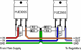 Fig.2 Construction Suggestion
Connect to a suitable power supply - remember that the supply earth (ground) must be connected! When powering up for the first time, use 100 ohm to 560 ohm "safety" resistors in series with each supply to limit the current if you have made a mistake in the wiring. There is very little that can go wrong (other than wiring mistakes), so any fault you may find is easily rectified.
Source: http://sound.westhost.com/project102.htm