Home » Circuits
Spike Detector For Oscilloscopes
Dynamic flip-flops ignore pulses at their inputs that are shorter than 40 ns or do not have TTL levels. This means that TTL flip-flops are poorly suited to capturing noise pulses having unknown durations and magnitudes. Anyone who has ever tried to observe very short laser pulses (15–25 ns) is familiar with this problem. By contrast, this circuit can detect impulses with widths less than 8 ns and amplitudes between +100 mV and +5 V. The heart of this circuit is formed by a MAX903, a very fast comparator with internal memory. The IC has separate supply pins for its analogue and digital portions. The analogue portion is powered by a symmetrical ±5-V supply.This allows the detector to also handle input voltages that are negative relative to ground. The internal memory and output stage operate from a single-ended +5-V supply, so the output signal has proper TTL levels. The MAX903 (IC1) has a special internal memory circuit (latch). The latch either connects the output of the internal comparator directly to the signal output or stores the most recent TTL level and blocks the output of the internal comparator, causing the most recent TTL level appears at the output. This allows short input pulses to be stretched to any desired length. Despite its extremely short switching times, the MAX903 consumes only a modest 18 mW.
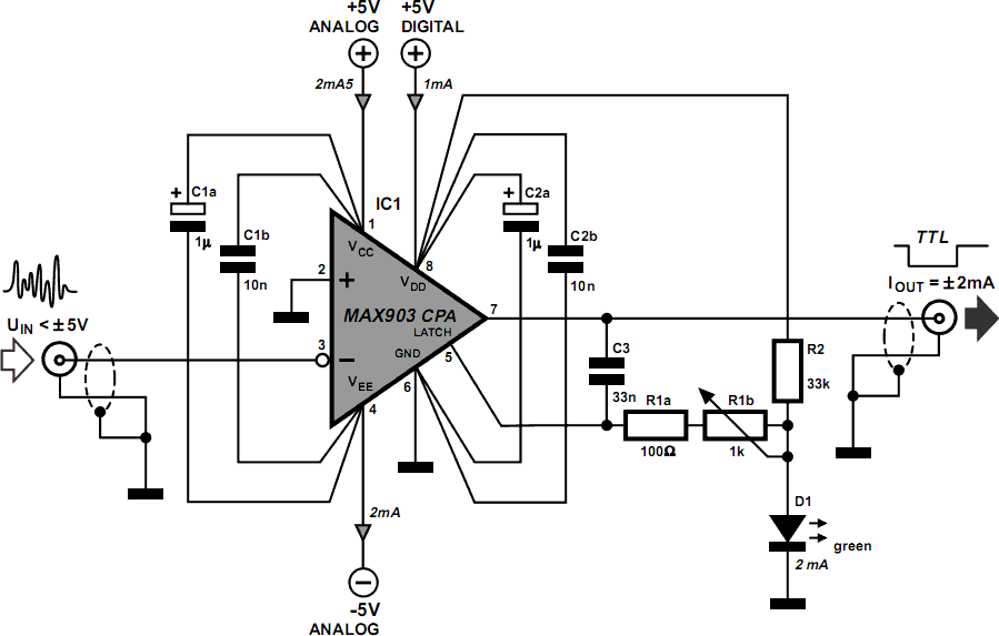
In the quiescent state, the voltage on the Latch input (pin 5) is at 1.75 V. This reference voltage is provided by LED D1, which draws its current via R2. In this state the latch is transparent, and a positive edge at the input appears will appear as a negative transition on the output after a propagation delay of 8 ns (tPD). This only happens if the peak voltage on the input is more positive than ground potential. C1 passes this change in the output voltage level to the Latch input (pin 5). As soon as the voltage on the Latch input drops below 1.4 V, the internal latch switches to the Hold state. In this state, the output is no longer connected to the comparator, and the output remains low for the duration of the latch hold time, regardless of what happens with the input signal.
The latch hold time is determined by the time constant of the C3/R1 network; it has an adjustment range of 100–500 ns. Pulses of this length can be readily observed using practically any oscilloscope. This latch function in this circuit is only triggered if the input signal has a rising edge that crosses the zero-voltage level. The internal latch remains transparent for signals in the range of –5 V to 0 V, so such pulses will not be stretched. If only positive input voltages are anticipated, the negative supply voltage is not necessary and the circuit can be powered from a single +5-V supply. A fast circuit such as this requires a carefully designed circuit board layout. All connections to the IC must be kept very short.
Decoupling capacitors C1 and C2 should preferably be placed immediately adjacent to the supply pins. Pin 3 of the IC can be bent upward and soldered directly to a length of coax or twisted-pair cable (air is still the best insulator). If a coax cable is used, the unbraided screen must not be formed into a long pigtail. It’s better to peel back a short length of the screen, wrap a length of bare wire around it and solder it directly to the ground plane. The supply traces for the analogue and digital portions must be well separated from each other, and each supply must be well decoupled, even if only a single supply voltage (+5 V) is used. The preferred solution is to use two independent voltage regulators.