Bipolar junction transistors
The bipolar transistor (BJT) was named because its operation involves conduction by two carriers: electrons and holes in the same crystal. The first bipolar transistor was invented at Bell Labs by William Shockley, Walter Brattain, and John Bardeen so late in 1947 that it was not published until 1948. Thus, many texts differ as to the date of invention. Brattain fabricated a germanium point contact transistor, bearing some resemblance to a point contact diode. Within a month, Shockley had a more practical junction transistor, which we describe in following paragraphs. They were awarded the Nobel Prize in Physics in 1956 for the transistor.
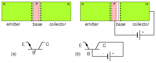
The bipolar junction transistor shown in Figure below(a) is an NPN three layer semiconductor sandwich with an emitter and collector at the ends, and a base in between. It is as if a third layer were added to a two layer diode. If this were the only requirement, we would have no more than a pair of back-to-back diodes. In fact, it is far easier to build a pair of back-to-back diodes. The key to the fabrication of a bipolar junction transistor is to make the middle layer, the base, as thin as possible without shorting the outside layers, the emitter and collector. We cannot over emphasize the importance of the thin base region.
The device in Figure below(a) has a pair of junctions, emitter to base and base to collector, and two depletion regions.

(a) NPN junction bipolar transistor. (b) Apply reverse bias to collector base junction.
It is customary to reverse bias the base-collector junction of a bipolar junction transistor as shown in (Figure above(b). Note that this increases the width of the depletion region. The reverse bias voltage could be a few volts to tens of volts for most transistors. There is no current flow, except leakage current, in the collector circuit.
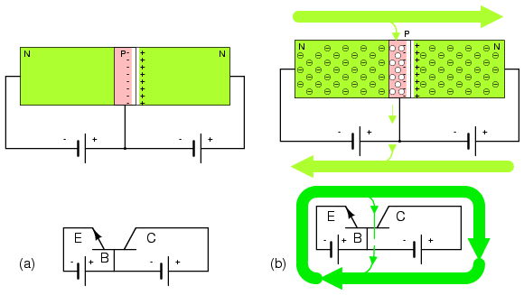
In Figure below(a), a voltage source has been added to the emitter base circuit. Normally we forward bias the emitter-base junction, overcoming the 0.6 V potential barrier. This is similar to forward biasing a junction diode. This voltage source needs to exceed 0.6 V for majority carriers (electrons for NPN) to flow from the emitter into the base becoming minority carriers in the P-type semiconductor.
If the base region were thick, as in a pair of back-to-back diodes, all the current entering the base would flow out the base lead. In our NPN transistor example, electrons leaving the emitter for the base would combine with holes in the base, making room for more holes to be created at the (+) battery terminal on the base as electrons exit.
However, the base is manufactured thin. A few majority carriers in the emitter, injected as minority carriers into the base, actually recombine. See Figure below(b). Few electrons injected by the emitter into the base of an NPN transistor fall into holes. Also, few electrons entering the base flow directly through the base to the positive battery terminal. Most of the emitter current of electrons diffuses through the thin base into the collector. Moreover, modulating the small base current produces a larger change in collector current. If the base voltage falls below approximately 0.6 V for a silicon transistor, the large emitter-collector current ceases to flow.

NPN junction bipolar transistor with reverse biased collector-base: (a) Adding forward bias to base-emitter junction, results in (b) a small base current and large emitter and collector currents.
In Figure below we take a closer look at the current amplification mechanism. We have an enlarged view of an NPN junction transistor with emphasis on the thin base region. Though not shown, we assume that external voltage sources 1) forward bias the emitter-base junction, 2) reverse bias the base-collector junction. Electrons, majority carriers, enter the emitter from the (-) battery terminal. The base current flow corresponds to electrons leaving the base terminal for the (+) battery terminal. This is but a small current compared to the emitter current.

Disposition of electrons entering base: (a) Lost due to recombination with base holes. (b) Flows out base lead. (c) Most diffuse from emitter through thin base into base-collector depletion region, and (d) are rapidly swept by the strong depletion region electric field into the collector.
Majority carriers within the N-type emitter are electrons, becoming minority carriers when entering the P-type base. These electrons face four possible fates entering the thin P-type base. A few at Figure above(a) fall into holes in the base that contributes to base current flow to the (+) battery terminal. Not shown, holes in the base may diffuse into the emitter and combine with electrons, contributing to base terminal current. Few at (b) flow on through the base to the (+) battery terminal as if the base were a resistor. Both (a) and (b) contribute to the very small base current flow. Base current is typically 1% of emitter or collector current for small signal transistors. Most of the emitter electrons diffuse right through the thin base (c) into the base-collector depletion region. Note the polarity of the depletion region surrounding the electron at (d). The strong electric field sweeps the electron rapidly into the collector. The strength of the field is proportional to the collector battery voltage. Thus 99% of the emitter current flows into the collector. It is controlled by the base current, which is 1% of the emitter current. This is a potential current gain of 99, the ratio of IC/IB, also known as beta, β.
This magic, the diffusion of 99% of the emitter carriers through the base, is only possible if the base is very thin. What would be the fate of the base minority carriers in a base 100 times thicker? One would expect the recombination rate, electrons falling into holes, to be much higher. Perhaps 99%, instead of 1%, would fall into holes, never getting to the collector. The second point to make is that the base current may control 99% of the emitter current, only if 99% of the emitter current diffuses into the collector. If it all flows out the base, no control is possible.
Another feature accounting for passing 99% of the electrons from emitter to collector is that real bipolar junction transistors use a small heavily doped emitter. The high concentration of emitter electrons forces many electrons to diffuse into the base. The lower doping concentration in the base means fewer holes diffuse into the emitter, which would increase the base current. Diffusion of carriers from emitter to base is strongly favored.
The thin base and the heavily doped emitter help keep the emitter efficiency high, 99% for example. This corresponds to 100% emitter current splitting between the base as 1% and the collector as 99%. The emitter efficiency is known as α = IC/IE.
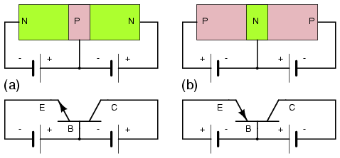
Bipolar junction transistors are available as PNP as well as NPN devices. We present a comparison of these two in Figure below. The difference is the polarity of the base emitter diode junctions, as signified by the direction of the schematic symbol emitter arrow. It points in the same direction as the anode arrow for a junction diode, against electron current flow. See diode junction, Figure previous. The point of the arrow and bar correspond to P-type and N-type semiconductors, respectively. For NPN and PNP emitters, the arrow points away and toward the base respectively. There is no schematic arrow on the collector. However, the base-collector junction is the same polarity as the base-emitter junction compared to a diode. Note, we speak of diode, not power supply, polarity.

Compare NPN transistor at (a) with the PNP transistor at (b). Note direction of emitter arrow and supply polarity.
The voltage sources for PNP transistors are reversed compared with an NPN transistors as shown in Figure above. The base-emitter junction must be forward biased in both cases. The base on a PNP transistor is biased negative (b) compared with positive (a) for an NPN. In both cases the base-collector junction is reverse biased. The PNP collector power supply is negative campared with positive for an NPN transistor.

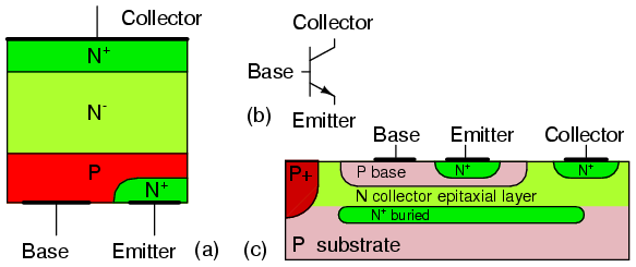
Bipolar junction transistor: (a) discrete device cross-section, (b) schematic symbol, (c) integrated circuit cross-section.
Note that the BJT in Figure above(a) has heavy doping in the emitter as indicated by the N+ notation. The base has a normal P-dopant level. The base is much thinner than the not-to-scale cross-section shows. The collector is lightly doped as indicated by the N- notation. The collector needs to be lightly doped so that the collector-base junction will have a high breakdown voltage. This translates into a high allowable collector power supply voltage. Small signal silicon transistors have a 60-80 V breakdown voltage. Though, it may run to hundreds of volts for high voltage transistors. The collector also needs to be heavily doped to minimize ohmic losses if the transistor must handle high current. These contradicting requirements are met by doping the collector more heavily at the metallic contact area. The collector near the base is lightly doped as compared with the emitter. The heavy doping in the emitter gives the emitter-base a low approximate 7 V breakdown voltage in small signal transistors. The heavily doped emitter makes the emitter-base junction have zener diode like characteristics in reverse bias.
The BJT die, a piece of a sliced and diced semiconductor wafer, is mounted collector down to a metal case for power transistors. That is, the metal case is electrically connected to the collector. A small signal die may be encapsulated in epoxy. In power transistors, aluminum bonding wires connect the base and emitter to package leads. Small signal transistor dies may be mounted directly to the lead wires. Multiple transistors may be fabricated on a single die called an integrated circuit. Even the collector may be bonded out to a lead instead of the case. The integrated circuit may contain internal wiring of the transistors and other integrated components. The integrated BJT shown in (Figure (c) above) is much thinner than the “not to scale” drawing. The P+ region isolates multiple transistors in a single die. An aluminum metalization layer (not shown) interconnects multiple transistors and other components. The emitter region is heavily doped, N+ compared to the base and collector to improve emitter efficiency.
Discrete PNP transistors are almost as high quality as the NPN counterpart. However, integrated PNP transistors are not nearly a good as the NPN variety within the same integrated circuit die. Thus, integrated circuits use the NPN variety as much as possible.
- REVIEW:
- Bipolar transistors conduct current using both electrons and holes in the same device.
- Operation of a bipolar transistor as a current amplifier requires that the collector-base junction be reverse biased and the emitter-base junction be forward biased.
- A transistor differs from a pair of back to back diodes in that the base, the center layer, is very thin. This allows majority carriers from the emitter to diffuse as minority carriers through the base into the depletion region of the base-collector junction, where the strong electric field collects them.
- Emitter efficiency is improved by heavier doping compared with the collector. Emitter efficiency: α = IC/IE, 0.99 for small signal devices
- Current gain is β=IC/IB, 100 to 300 for small signal transistors.
