The common-emitter amplifier
At the beginning of this chapter we saw how transistors could be used as switches, operating in either their "saturation" or "cutoff" modes. In the last section we saw how transistors behave within their "active" modes, between the far limits of saturation and cutoff. Because transistors are able to control current in an analog (infinitely divisible) fashion, they find use as amplifiers for analog signals.
One of the simpler transistor amplifier circuits to study is the one used previously for illustrating the transistor's switching ability:
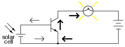
It is called the common-emitter configuration because (ignoring the power supply battery) both the signal source and the load share the emitter lead as a common connection point. This is not the only way in which a transistor may be used as an amplifier, as we will see in later sections of this chapter:
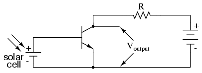
Before, this circuit was shown to illustrate how a relatively small current from a solar cell could be used to saturate a transistor, resulting in the illumination of a lamp. Knowing now that transistors are able to "throttle" their collector currents according to the amount of base current supplied by an input signal source, we should be able to see that the brightness of the lamp in this circuit is controllable by the solar cell's light exposure. When there is just a little light shone on the solar cell, the lamp will glow dimly. The lamp's brightness will steadily increase as more light falls on the solar cell.
Suppose that we were interested in using the solar cell as a light intensity instrument. We want to be able to measure the intensity of incident light with the solar cell by using its output current to drive a meter movement. It is possible to directly connect a meter movement to a solar cell for this purpose. In fact, the simplest light-exposure meters for photography work are designed like this:
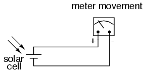
While this approach might work for moderate light intensity measurements, it would not work as well for low light intensity measurements. Because the solar cell has to supply the meter movement's power needs, the system is necessarily limited in its sensitivity. Supposing that our need here is to measure very low-level light intensities, we are pressed to find another solution.
Perhaps the most direct solution to this measurement problem is to use a transistor to amplify the solar cell's current so that more meter movement needle deflection may be obtained for less incident light. Consider this approach:
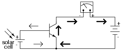
Current through the meter movement in this circuit will be β times the solar cell current. With a transistor β of 100, this represents a substantial increase in measurement sensitivity. It is prudent to point out that the additional power to move the meter needle comes from the battery on the far right of the circuit, not the solar cell itself. All the solar cell's current does is control battery current to the meter to provide a greater meter reading than the solar cell could provide unaided.
Because the transistor is a current-regulating device, and because meter movement indications are based on the amount of current through their movement coils, meter indication in this circuit should depend only on the amount of current from the solar cell, not on the amount of voltage provided by the battery. This means the accuracy of the circuit will be independent of battery condition, a significant feature! All that is required of the battery is a certain minimum voltage and current output ability to be able to drive the meter full-scale if needed.
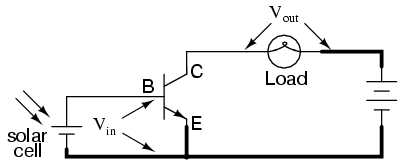
Another way in which the common-emitter configuration may be used is to produce an output voltage derived from the input signal, rather than a specific output current. Let's replace the meter movement with a plain resistor and measure voltage between collector and emitter:
With the solar cell darkened (no current), the transistor will be in cutoff mode and behave as an open switch between collector and emitter. This will produce maximum voltage drop between collector and emitter for maximum Voutput, equal to the full voltage of the battery.
At full power (maximum light exposure), the solar cell will drive the transistor into saturation mode, making it behave like a closed switch between collector and emitter. The result will be minimum voltage drop between collector and emitter, or almost zero output voltage. In actuality, a saturated transistor can never achieve zero voltage drop between collector and emitter due to the two PN junctions through which collector current must travel. However, this "collector-emitter saturation voltage" will be fairly low, around several tenths of a volt, depending on the specific transistor used.
For light exposure levels somewhere between zero and maximum solar cell output, the transistor will be in its active mode, and the output voltage will be somewhere between zero and full battery voltage. An important quality to note here about the common-emitter configuration is that the output voltage is inversely proportional to the input signal strength. That is, the output voltage decreases as the input signal increases. For this reason, the common-emitter amplifier configuration is referred to as an inverting amplifier.
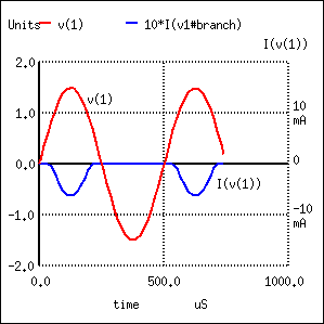
A quick SPICE simulation will verify our qualitative conclusions about this amplifier circuit:
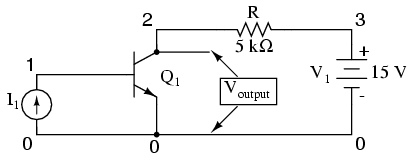
common-emitter amplifier
i1 0 1 dc
q1 2 1 0 mod1
r 3 2 5000
v1 3 0 dc 15
.model mod1 npn
.dc i1 0 50u 2u
.plot dc v(2,0)
.end
type        npn
is        1.00E-16
bf         100.000
nf           1.000
br           1.000
nr           1.000
The simulation plots both the input voltage (an AC signal of 1.5 volt peak amplitude and 2000 Hz frequency) and the current through the 15 volt battery, which is the same as the current through the speaker. What we see here is a full AC sine wave alternating in both positive and negative directions, and a half-wave output current waveform that only pulses in one direction. If we were actually driving a speaker with this waveform, the sound produced would be horribly distorted.
What's wrong with the circuit? Why won't it faithfully reproduce the entire AC waveform from the microphone? The answer to this question is found by close inspection of the transistor diode-regulating diode model:
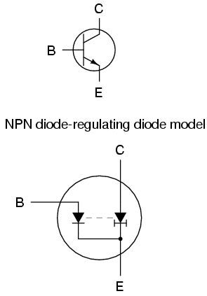
Collector current is controlled, or regulated, through the constant-current mechanism according to the pace set by the current through the base-emitter diode. Note that both current paths through the transistor are monodirectional: one way only! Despite our intent to use the transistor to amplify an AC signal, it is essentially a DC device, capable of handling currents in a single direction only. We may apply an AC voltage input signal between the base and emitter, but electrons cannot flow in that circuit during the part of the cycle that reverse-biases the base-emitter diode junction. Therefore, the transistor will remain in cutoff mode throughout that portion of the cycle. It will "turn on" in its active mode only when the input voltage is of the correct polarity to forward-bias the base-emitter diode, and only when that voltage is sufficiently high to overcome the diode's forward voltage drop. Remember that bipolar transistors are current-controlled devices: they regulate collector current based on the existence of base-to-emitter current, not base-to-emitter voltage.
The only way we can get the transistor to reproduce the entire waveform as current through the speaker is to keep the transistor in its active mode the entire time. This means we must maintain current through the base during the entire input waveform cycle. Consequently, the base-emitter diode junction must be kept forward-biased at all times. Fortunately, this can be accomplished with the aid of a DC bias voltage added to the input signal. By connecting a sufficient DC voltage in series with the AC signal source, forward-bias can be maintained at all points throughout the wave cycle:
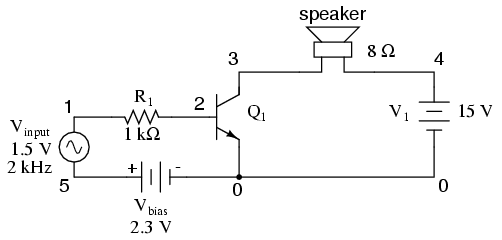
common-emitter amplifier
vinput 1 5 sin (0 1.5 2000 0 0)
vbias 5 0 dc 2.3
r1 1 2 1k
q1 3 2 0 mod1
rspkr 3 4 8
v1 4 0 dc 15
.model mod1 npn
.tran 0.02m 0.78m
.plot tran v(1,0) i(v1)
.end
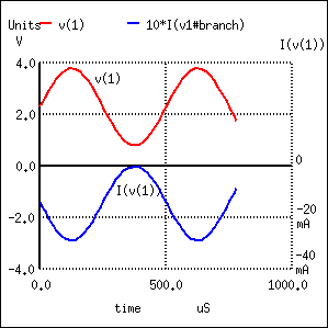
With the bias voltage source of 2.3 volts in place, the transistor remains in its active mode throughout the entire cycle of the wave, faithfully reproducing the waveform at the speaker. Notice that the input voltage (measured between nodes 1 and 0) fluctuates between about 0.8 volts and 3.8 volts, a peak-to-peak voltage of 3 volts just as expected (source voltage = 1.5 volts peak). The output (speaker) current varies between zero and almost 300 mA, 180o out of phase with the input (microphone) signal.
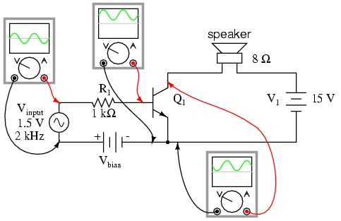
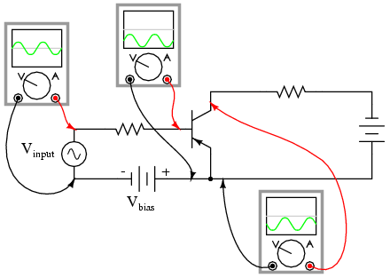
The following illustration is another view of the same circuit, this time with a few oscilloscopes ("scopemeters") connected at crucial points to display all the pertinent signals:
The need for biasing a transistor amplifier circuit to obtain full waveform reproduction is an important consideration. A separate section of this chapter will be devoted entirely to the subject biasing and biasing techniques. For now, it is enough to understand that biasing may be necessary for proper voltage and current output from the amplifier.
Now that we have a functioning amplifier circuit, we can investigate its voltage, current, and power gains. The generic transistor used in these SPICE analyses has a β of 100, as indicated by the short transistor statistics printout included in the text output (these statistics were cut from the last two analyses for brevity's sake):
type        npn
is        1.00E-16
bf         100.000
nf           1.000
br           1.000
nr           1.000
β is listed under the abbreviation "bf," which actually stands for "beta, forward". If we wanted to insert our own β ratio for an analysis, we could have done so on the .model line of the SPICE netlist.
Since β is the ratio of collector current to base current, and we have our load connected in series with the collector terminal of the transistor and our source connected in series with the base, the ratio of output current to input current is equal to beta. Thus, our current gain for this example amplifier is 100, or 40 dB.
Voltage gain is a little more complicated to figure than current gain for this circuit. As always, voltage gain is defined as the ratio of output voltage divided by input voltage. In order to experimentally determine this, we need to modify our last SPICE analysis to plot output voltage rather than output current so we have two voltage plots to compare:
common-emitter amplifier
vinput 1 5 sin (0 1.5 2000 0 0)
vbias 5 0 dc 2.3
r1 1 2 1k
q1 3 2 0 mod1
rspkr 3 4 8
v1 4 0 dc 15
.model mod1 npn
.tran 0.02m 0.78m
.plot tran v(1,0) v(4,3)
.end
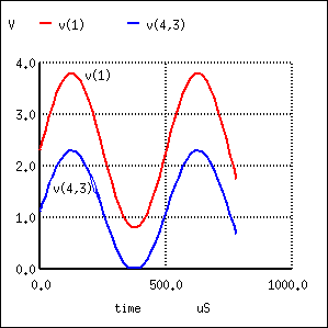
Plotted on the same scale (from 0 to 4 volts), we see that the output waveform ("+") has a smaller peak-to-peak amplitude than the input waveform ("*"), in addition to being at a lower bias voltage, not elevated up from 0 volts like the input. Since voltage gain for an AC amplifier is defined by the ratio of AC amplitudes, we can ignore any DC bias separating the two waveforms. Even so, the input waveform is still larger than the output, which tells us that the voltage gain is less than 1 (a negative dB figure).
To be honest, this low voltage gain is not characteristic to all common-emitter amplifiers. In this case it is a consequence of the great disparity between the input and load resistances. Our input resistance (R1) here is 1000 Ω, while the load (speaker) is only 8 Ω. Because the current gain of this amplifier is determined solely by the β of the transistor, and because that β figure is fixed, the current gain for this amplifier won't change with variations in either of these resistances. However, voltage gain is dependent on these resistances. If we alter the load resistance, making it a larger value, it will drop a proportionately greater voltage for its range of load currents, resulting in a larger output waveform. Let's try another simulation, only this time with a 30 Ω load instead of an 8 Ω load:
common-emitter amplifier
vinput 1 5 sin (0 1.5 2000 0 0)
vbias 5 0 dc 2.3
r1 1 2 1k
q1 3 2 0 mod1
rspkr 3 4 30
v1 4 0 dc 15
.model mod1 npn
.tran 0.02m 0.78m
.plot tran v(1,0) v(4,3)
.end
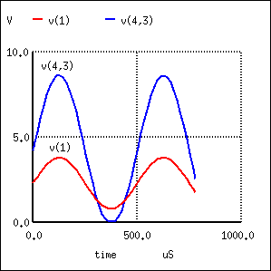
This time the output voltage waveform is significantly greater in amplitude than the input waveform. Looking closely, we can see that the output waveform ("+") crests between 0 and about 9 volts: approximately 3 times the amplitude of the input voltage.
We can perform another computer analysis of this circuit, only this time instructing SPICE to analyze it from an AC point of view, giving us peak voltage figures for input and output instead of a time-based plot of the waveforms:
common-emitter amplifier
vinput 1 5 ac 1.5
vbias 5 0 dc 2.3
r1 1 2 1k
q1 3 2 0 mod1
rspkr 3 4 30
v1 4 0 dc 15
.model mod1 npn
.ac lin 1 2000 2000
.print ac v(1,0) v(4,3)
.end
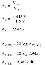
freq          v(1)        v(4,3)
2.000E+03     1.500E+00   4.418E+00
Peak voltage measurements of input and output show an input of 1.5 volts and an output of 4.418 volts. This gives us a voltage gain ratio of 2.9453 (4.418 V / 1.5 V), or 9.3827 dB.
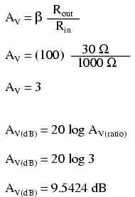
Because the current gain of the common-emitter amplifier is fixed by β, and since the input and output voltages will be equal to the input and output currents multiplied by their respective resistors, we can derive an equation for approximate voltage gain:
As you can see, the predicted results for voltage gain are quite close to the simulated results. With perfectly linear transistor behavior, the two sets of figures would exactly match. SPICE does a reasonable job of accounting for the many "quirks" of bipolar transistor function in its analysis, hence the slight mismatch in voltage gain based on SPICE's output.
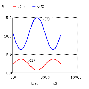
These voltage gains remain the same regardless of where we measure output voltage in the circuit: across collector and emitter, or across the series load resistor as we did in the last analysis. The amount of output voltage change for any given amount of input voltage will remain the same. Consider the two following SPICE analyses as proof of this. The first simulation is time-based, to provide a plot of input and output voltages. You will notice that the two signals are 180o out of phase with each other. The second simulation is an AC analysis, to provide simple, peak voltage readings for input and output:
common-emitter amplifier
vinput 1 5 sin (0 1.5 2000 0 0)
vbias 5 0 dc 2.3
r1 1 2 1k
q1 3 2 0 mod1
rspkr 3 4 30
v1 4 0 dc 15
.model mod1 npn
.tran 0.02m 0.74m
.plot tran v(1,0) v(3,0)
.end
common-emitter amplifier
vinput 1 5 ac 1.5
vbias 5 0 dc 2.3
r1 1 2 1k
q1 3 2 0 mod1
rspkr 3 4 30
v1 4 0 dc 15
.model mod1 npn
.ac lin 1 2000 2000
.print ac v(1,0) v(3,0)
.end
freq          v(1)        v(3)
2.000E+03     1.500E+00   4.418E+00
We still have a peak output voltage of 4.418 volts with a peak input voltage of 1.5 volts. The only difference from the last set of simulations is the phase of the output voltage.
So far, the example circuits shown in this section have all used NPN transistors. PNP transistors are just as valid to use as NPN in any amplifier configuration, so long as the proper polarity and current directions are maintained, and the common-emitter amplifier is no exception. The inverting behavior and gain properties of a PNP transistor amplifier are the same as its NPN counterpart, just the polarities are different:
- REVIEW:
- Common-emitter transistor amplifiers are so-called because the input and output voltage points share the emitter lead of the transistor in common with each other, not considering any power supplies.
- Transistors are essentially DC devices: they cannot directly handle voltages or currents that reverse direction. In order to make them work for amplifying AC signals, the input signal must be offset with a DC voltage to keep the transistor in its active mode throughout the entire cycle of the wave. This is called biasing.
- If the output voltage is measured between emitter and collector on a common-emitter amplifier, it will be 180o out of phase with the input voltage waveform. For this reason, the common-emitter amplifier is called an inverting amplifier circuit.
- The current gain of a common-emitter transistor amplifier with the load connected in series with the collector is equal to β. The voltage gain of a common-emitter transistor amplifier is approximately given here:
-
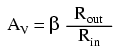
- Where "Rout" is the resistor connected in series with the collector and "Rin" is the resistor connected in series with the base.