Radio circuits -- INCOMPLETE
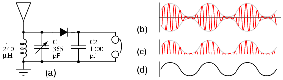
(a) Crystal radio. (b) Modulated RF at antenna. (c) Rectified RF at diode cathode, without C2 filter capacitor. (d) Demodualted audio to headphones.
An antenna ground system, tank circuit, peak detector, and headphones are the the main components of a crystal radio. See Figure above (a). The antenna absorbs transimtted radio signals (b) which flow to ground via the other components. The combination of C1 and L1 comprise a resonant circuit, refered to as a tank circuit. Its purpose is to select one out of many available radios signals. The variable capacitor C1 allows for tuning to the various signals. The diode passes the positive half cycles of the RF, removing the negative half cycles (c). C2 is sized to filter the radio frequencies from the RF envelope (c), passing audio frequencies (d) to the headset. Note that no power supply is required for a crystal radio. A germanium diode, which has a lower forward voltage drop provides greater sensitvity than a silicon diode.
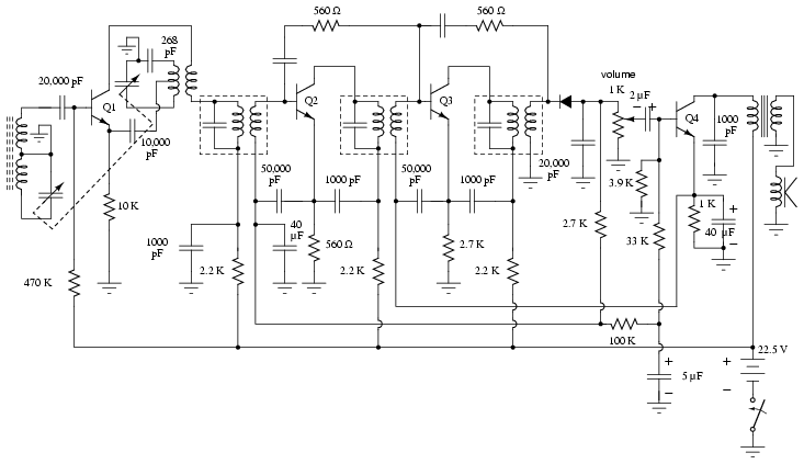
Regency TR1: First mass produced transistor radio, 1954.
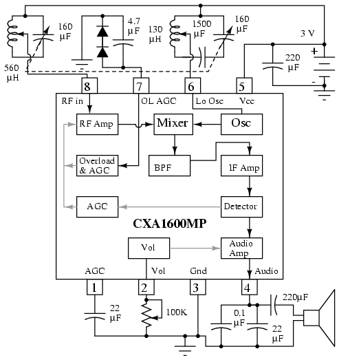
The circuit in Figure below is an integrated circuit AM radio containing all the active radio frequency circuitry within a single IC. All capacitors and inductors, along with a few resistors, are external to the IC. The 370 Pf variable capacitor tunes the desired RF signal. The 320 pF variable capacitor tunes the local oscillator 455 KHz above the RF input signal. The RF signal and local oscillator frequencies mix producing the sun and difference of the two at pin 15. The external 455 KHz ceramic filter between pins 15 and 12, selects the 455 KHz difference frequency. Most of the amplification is in the intermediate frequency (IF) amplifier between pins 12 and 7. A diode at pin 7 recovers audio from the IF. Some automatic gain control (AGC) is recovered and filtered to DC and fed back into pin 9.
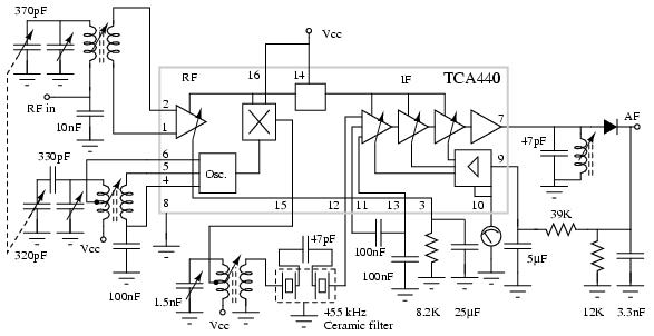
IC radio, After Signetics [SIG]
Figure below shows conventional mecahnical tuning (a) of the RF input tuner and the local oscillator with varactor diode tuning (b). The meshed plates of a dual variable capacitor make for a bulky component. It is ecconomic to replace it with varicap tuning diodes. Increasing the reverse bias Vtune decreases capacitance which increases frequency. Vtune could be produced by a potentiometer.
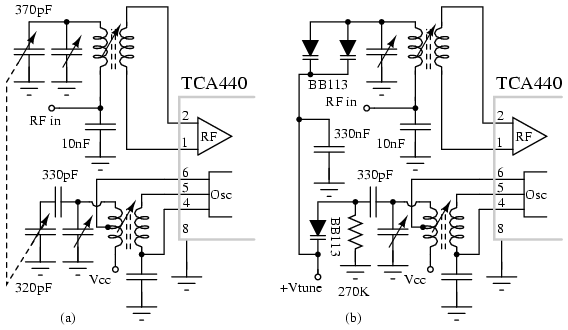
IC radio comparison of (a) mechanical tuning to (b) electronic varicap diode tuning.[SIG]
Figure below shows an even lower parts count AM radio. Sony engineers have included the intermediate frequency (IF) bandpass filter within the 8-pin IC. This eliminates external IF transformers and an IF ceramic filter. L-C tuning components are still required for the radio frequency (RF) input and the local oscillator. Though, the variable capacitors could be replaced by varicap tuning diodes.
Compact IC radio eliminates external IF filters. After Sony [SNE]
Figure below is an example of a common-base (CB) RF amplifier. It is a good illustration because it looks like a CB for lack of a bias network. Since there is no bias, this is a class C amplifier. The transistor conducts for less than 180o of the input signal because at least 0.7 V bias would be required for 180o class B. The common-base configuration has higher power gain at high RF frequencies than common-emitter. This is a power amplifier (3/4 W) as opposed to a small signal amplifier. The input and output π-networks match the emitter and collector to the 50 Ω input and output coaxial terminations, respectively. The output π-network also helps filter harmonics generated by the class C amplifier. Though, more sections would likely be required by modern radiated emissions standards.
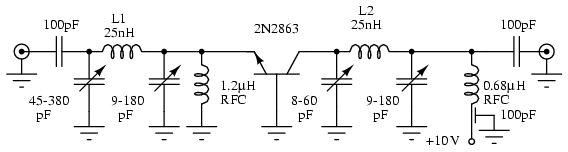
Class C common-base 750 mW RF power amplifier. L1 = #10 Cu wire 1/2 turn, 5/8 in. ID by 3/4 in. high. L2 = #14 tinned Cu wire 1 1/2 turns, 1/2 in. ID by 1/3 in. spacing. After Texas Instruments [TX1]
An example of a high gain common-base RF amplifier is shown in Figure below. The common-base circuit can be pushed to a higher frequency than other configurations. This is a common base configuration because the transistor bases are grounded for AC by 1000 pF capacitors. The capacitors are necessary (unlike the class C, Figure previous) to allow the 1KΩ-4KΩ voltage divider to bias the transistor base for class A operation. The 500Ω resistors are emitter bias resistors. They stablize the collector current. The 850Ω resistors are collector DC loads. The three stage amplifier provides an overall gain of 38 dB at 100 MHz with a 9 MHz bandwidth.
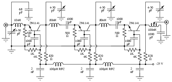
Class A common-base small-signal high gain amplifier. After Texas Instruments [TX2]
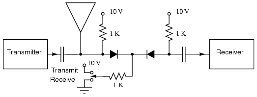
PIN diode T/R switch disconnects receiver from antenna during transmit.
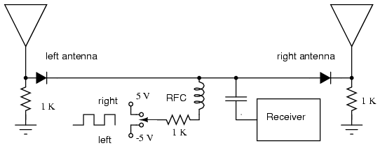
PIN diode antenna switch for direction finder receiver.
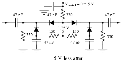
PIN diode attenuator: PIN diodes function as voltage variable resistors. After Lin [LCC].
The PIN diodes are arranged in a π-attenuator network. The anti-series diodes cancel some harmonic distortion compared with a single series diode. The fixed 1.25 V supply forward biases the parallel diodes, which not only conducting DC current from ground via the resistors, but also, conduct RF to ground through the diodes' capacitors. The control voltage Vcontrol, increases current through the parallel diodes as it increases. This decreases the resistance and attenuation, passing more RF from input to output. Attenuation is about 3 dB at Vcontrol= 5 V. Attenuation is 40 dB at Vcontrol= 1 V with flat frequency response to 2 gHz. At Vcontrol= 0.5 V, attenuation is 80 dB at 10 MHz. However, the frequency response varies too much to use. [LCC]