Introduction
Shift registers, like counters, are a form of sequential logic. Sequential logic, unlike combinational logic is not only affected by the present inputs, but also, by the prior history. In other words, sequential logic remembers past events.
Shift registers produce a discrete delay of a digital signal or waveform. A waveform synchronized to a clock, a repeating square wave, is delayed by "n" discrete clock times, where "n" is the number of shift register stages. Thus, a four stage shift register delays "data in" by four clocks to "data out". The stages in a shift register are delay stages, typically type "D" Flip-Flops or type "JK" Flip-flops.
Formerly, very long (several hundred stages) shift registers served as digital memory. This obsolete application is reminiscent of the acoustic mercury delay lines used as early computer memory.
Serial data transmission, over a distance of meters to kilometers, uses shift registers to convert parallel data to serial form. Serial data communications replaces many slow parallel data wires with a single serial high speed circuit.
Serial data over shorter distances of tens of centimeters, uses shift registers to get data into and out of microprocessors. Numerous peripherals, including analog to digital converters, digital to analog converters, display drivers, and memory, use shift registers to reduce the amount of wiring in circuit boards.
Some specialized counter circuits actually use shift registers to generate repeating waveforms. Longer shift registers, with the help of feedback generate patterns so long that they look like random noise, pseudo-noise.
Basic shift registers are classified by structure according to the following types:
- Serial-in/serial-out
- Parallel-in/serial-out
- Serial-in/parallel-out
- Universal parallel-in/parallel-out
- Ring counter
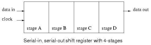
Above we show a block diagram of a serial-in/serial-out shift register, which is 4-stages long. Data at the input will be delayed by four clock periods from the input to the output of the shift register.
Data at "data in", above, will be present at the Stage A output after the first clock pulse. After the second pulse stage A data is transfered to stage B output, and "data in" is transfered to stage A output. After the third clock, stage C is replaced by stage B; stage B is replaced by stage A; and stage A is replaced by "data in". After the fourth clock, the data originally present at "data in" is at stage D, "output". The "first in" data is "first out" as it is shifted from "data in" to "data out".
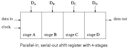
Data is loaded into all stages at once of a parallel-in/serial-out shift register. The data is then shifted out via "data out" by clock pulses. Since a 4- stage shift register is shown above, four clock pulses are required to shift out all of the data. In the diagram above, stage D data will be present at the "data out" up until the first clock pulse; stage C data will be present at "data out" between the first clock and the second clock pulse; stage B data will be present between the second clock and the third clock; and stage A data will be present between the third and the fourth clock. After the fourth clock pulse and thereafter, successive bits of "data in" should appear at "data out" of the shift register after a delay of four clock pulses.
If four switches were connected to DA through DD, the status could be read into a microprocessor using only one data pin and a clock pin. Since adding more switches would require no additional pins, this approach looks attractive for many inputs.
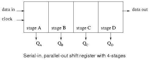
Above, four data bits will be shifted in from "data in" by four clock pulses and be available at QA through QD for driving external circuitry such as LEDs, lamps, relay drivers, and horns.
After the first clock, the data at "data in" appears at QA. After the second clock, The old QA data appears at QB; QA receives next data from "data in". After the third clock, QB data is at QC. After the fourth clock, QC data is at QD. This stage contains the data first present at "data in". The shift register should now contain four data bits.
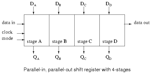
A parallel-in/laralel-out shift register combines the function of the parallel-in, serial-out shift register with the function of the serial-in, parallel-out shift register to yields the universal shift register. The "do anything" shifter comes at a price– the increased number of I/O (Input/Output) pins may reduce the number of stages which can be packaged.
Data presented at DA through DD is parallel loaded into the registers. This data at QA through QD may be shifted by the number of pulses presented at the clock input. The shifted data is available at QA through QD. The "mode" input, which may be more than one input, controls parallel loading of data from DA through DD, shifting of data, and the direction of shifting. There are shift registers which will shift data either left or right.
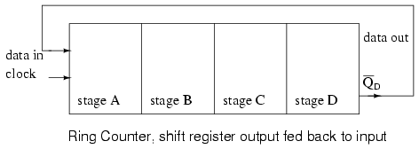
If the serial output of a shift register is connected to the serial input, data can be perpetually shifted around the ring as long as clock pulses are present. If the output is inverted before being fed back as shown above, we do not have to worry about loading the initial data into the "ring counter".