Bipolar junction transistor theory
Question 1:
| Don't just sit there! Build something!! |
Learning to mathematically analyze circuits requires much study and practice. Typically, students practice by working through lots of sample problems and checking their answers against those provided by the textbook or the instructor. While this is good, there is a much better way.
You will learn much more by actually building and analyzing real circuits, letting your test equipment provide the änswers" instead of a book or another person. For successful circuit-building exercises, follow these steps:
- 1.
- Carefully measure and record all component values prior to circuit construction, choosing resistor values high enough to make damage to any active components unlikely.
- 2.
- Draw the schematic diagram for the circuit to be analyzed.
- 3.
- Carefully build this circuit on a breadboard or other convenient medium.
- 4.
- Check the accuracy of the circuit's construction, following each wire to each connection point, and verifying these elements one-by-one on the diagram.
- 5.
- Mathematically analyze the circuit, solving for all voltage and current values.
- 6.
- Carefully measure all voltages and currents, to verify the accuracy of your analysis.
- 7.
- If there are any substantial errors (greater than a few percent), carefully check your circuit's construction against the diagram, then carefully re-calculate the values and re-measure.
When students are first learning about semiconductor devices, and are most likely to damage them by making improper connections in their circuits, I recommend they experiment with large, high-wattage components (1N4001 rectifying diodes, TO-220 or TO-3 case power transistors, etc.), and using dry-cell battery power sources rather than a benchtop power supply. This decreases the likelihood of component damage.
As usual, avoid very high and very low resistor values, to avoid measurement errors caused by meter "loading" (on the high end) and to avoid transistor burnout (on the low end). I recommend resistors between 1 kW and 100 kW.
One way you can save time and reduce the possibility of error is to begin with a very simple circuit and incrementally add components to increase its complexity after each analysis, rather than building a whole new circuit for each practice problem. Another time-saving technique is to re-use the same components in a variety of different circuit configurations. This way, you won't have to measure any component's value more than once.
Notes:
It has been my experience that students require much practice with circuit analysis to become proficient. To this end, instructors usually provide their students with lots of practice problems to work through, and provide answers for students to check their work against. While this approach makes students proficient in circuit theory, it fails to fully educate them.
Students don't just need mathematical practice. They also need real, hands-on practice building circuits and using test equipment. So, I suggest the following alternative approach: students should build their own "practice problems" with real components, and try to mathematically predict the various voltage and current values. This way, the mathematical theory "comes alive," and students gain practical proficiency they wouldn't gain merely by solving equations.
Another reason for following this method of practice is to teach students scientific method: the process of testing a hypothesis (in this case, mathematical predictions) by performing a real experiment. Students will also develop real troubleshooting skills as they occasionally make circuit construction errors.
Spend a few moments of time with your class to review some of the "rules" for building circuits before they begin. Discuss these issues with your students in the same Socratic manner you would normally discuss the worksheet questions, rather than simply telling them what they should and should not do. I never cease to be amazed at how poorly students grasp instructions when presented in a typical lecture (instructor monologue) format!
A note to those instructors who may complain about the "wasted" time required to have students build real circuits instead of just mathematically analyzing theoretical circuits:
What is the purpose of students taking your course?
If your students will be working with real circuits, then they should learn on real circuits whenever possible. If your goal is to educate theoretical physicists, then stick with abstract analysis, by all means! But most of us plan for our students to do something in the real world with the education we give them. The "wasted" time spent building real circuits will pay huge dividends when it comes time for them to apply their knowledge to practical problems.
Furthermore, having students build their own practice problems teaches them how to perform primary research, thus empowering them to continue their electrical/electronics education autonomously.
In most sciences, realistic experiments are much more difficult and expensive to set up than electrical circuits. Nuclear physics, biology, geology, and chemistry professors would just love to be able to have their students apply advanced mathematics to real experiments posing no safety hazard and costing less than a textbook. They can't, but you can. Exploit the convenience inherent to your science, and get those students of yours practicing their math on lots of real circuits!
Question 2:
The power dissipation of a transistor is given by the following equation:
|
Manipulate this equation to solve for beta, given all the other variables.
|
Notes:
Although this question is essentially nothing more than an exercise in algebraic manipulation, it is also a good lead-in to a discussion on the importance of power dissipation as a semiconductor device rating.
High temperature is the bane of most semiconductors, and high temperature is caused by excessive power dissipation. A classic example of this, though a bit dated, is the temperature sensitivity of the original germanium transistors. These devices were extremely sensitive to heat, and would fail rather quickly if allowed to overheat. Solid state design engineers had to be very careful in the techniques they used for transistor circuits to ensure their sensitive germanium transistors would not suffer from "thermal runaway" and destroy themselves.
Silicon is much more forgiving then germanium, but heat is still a problem with these devices. At the time of this writing (2004), there is promising developmental work on silicon carbide and gallium nitride transistor technology, which is able to function under much higher temperatures than silicon.
Question 3:
Suppose we only knew the emitter and base currents for an operating transistor and wished to calculate b from that information. We would need a definition of beta cast in terms of IE and IB instead of IC and IB.
Apply algebraic substitution to the formula b = [(IC)/(IB)] so that beta (b) is defined in terms of IE and IB. You may find the following equation helpful in your work:
|
|
Notes:
This question is nothing more than an exercise in algebraic manipulation.
Question 4:
A bipolar junction transistor parameter similar to b is älpha," symbolized by the Greek letter a. It is defined as the ratio between collector current and emitter current:
|
Apply algebraic substitution to this formula so that alpha is defined as a function of beta: a = f(b). In other words, substitute and manipulate this equation until you have alpha by itself on one side and no variable except beta on the other.
You may find the following equations helpful in your work:
|
|
Follow-up question: what range of values might you expect for a, with a typical transistor?
Notes:
This question is nothing more than an exercise in algebraic manipulation.
Question 5:
A technician uses a multimeter's "diode check" function to identify the terminals on a BJT. There are only two places where a non-infinite reading is obtained, and they are as follows:
|
|
From these measurements, determine what type of BJT this is (PNP or NPN) and identify all three terminals.
|
|
Notes:
It is a very useful skill to be able to identify a BJT using nothing more than the "diode check" function on a multimeter.
Question 6:
Conduction of an electric current through the collector terminal of a bipolar junction transistor requires that minority carriers be ïnjected" into the base region by a base-emitter current. Only after being injected into the base region may these charge carriers be swept toward the collector by the applied voltage between emitter and collector to constitute a collector current:
|
|
|
|
An analogy to help illustrate this is a person tossing flower petals into the air above their head, while a breeze carries the petals horizontally away from them. None of the flower petals may be ßwept" away by the breeze until the person releases them into the air, and the velocity of the breeze has no bearing on how many flower petals are swept away from the person, since they must be released from the person's grip before they can go anywhere.
By referencing either the energy diagram or the flower petal analogy, explain why the collector current for a BJT is strongly influenced by the base current and only weakly influenced by the collector-to-emitter voltage.
Notes:
This is one of my better analogies for explaining BJT operation, especially for illustrating the why IC is almost independent of VCE. It also helps to explain reverse recovery time for transistors: imagine how long it takes the air to clear of tossed flower petals after you stop tossing them, analogous to latent charge carriers having to be swept out of the base region by VCE after base current stops.
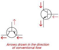
Question 7:
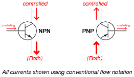
Bipolar junction transistor (BJT) function is usually considered in terms of currents: a relatively small current through one of the transistor's terminals exerts control over a much larger current. Draw the directions of all currents for these two transistors (one NPN and one PNP), clearly identifying which of the currents is doing the control, and which of the currents is being controlled:
|
|
|
|
Notes:
I have heard questions of this sort asked on technician job interviews. Knowing which way currents go through a BJT is considered a very fundamental aspect of electronics technician knowledge, and for good reason. It is impossible to understand the function of many transistor circuits without a firm grasp on which signal exerts control over which other signal in a circuit.
Question 8:
The "beta" ratio (b) of a bipolar junction transistor, sometimes alternatively referred to as hFE, is a very important device parameter. In essence, it describes the amplifying power of the transistor. Give a mathematical definition for this parameter, and provide some typical values from transistor datasheets.
- �
- 2N2222
- �
- 2N2905
- �
- 2N2907
- �
- 2N3403
- �
- 2N3703
- �
- 2N3904
- �
- 2N3906
- �
- 2N4125
- �
- 2N4403
- �
- 2N3055
- �
- TIP 29
- �
- TIP 31
- �
- TIP 32
- �
- TIP 41
- �
- TIP 42
Follow-up question #1: what conditions affect the b ratio of a transistor?
Follow-up question #2: re-write the b equation to solve for the other variables (IC = � , IB = �).
Notes:
Ask your students to show you at least one datasheets for one of the listed transistors. With internet access, datasheets are extremely easy to locate. Your students will need to be able to locate component datasheets and application notes as part of their work responsibilities, so be sure they know how and where to access these valuable documents!
The follow-up question is an important one to discuss, as b is far from stable for most transistors! This point is often overlooked in basic electronics textbooks, leaving students with the false impression that transistor circuit calculations using b are far more accurate than they actually are.
Question 9:
Find one or two real bipolar junction transistors and bring them with you to class for discussion. Identify as much information as you can about your transistors prior to discussion:
- �
- Terminal identification (which terminal is base, emitter, collector)
- �
- Continuous power rating
- �
- Typical b
Notes:
The purpose of this question is to get students to kinesthetically interact with the subject matter. It may seem silly to have students engage in a ßhow and tell" exercise, but I have found that activities such as this greatly help some students. For those learners who are kinesthetic in nature, it is a great help to actually touch real components while they're learning about their function. Of course, this question also provides an excellent opportunity for them to practice interpreting component markings, use a multimeter, access datasheets, etc.
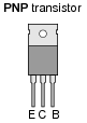
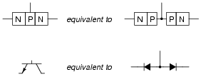
Question 10:
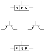
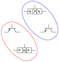
Match the following bipolar transistor illustrations to their respective schematic symbols:
|
|
|
|
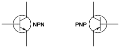
Follow-up question: identify the terminals on each transistor schematic symbol (base, emitter, and collector).
Notes:
Be sure to ask your students which of these transistor symbols represents the "NPN" type and which represents the "PNP" type. Although it will be obvious to most from the ßandwich" illustrations showing layers of "P" and "N" type material, this fact may escape the notice of a few students.
It might help to review diode symbols, if some students experience difficulty in matching the designations (PNP versus NPN) with the schematic symbols.
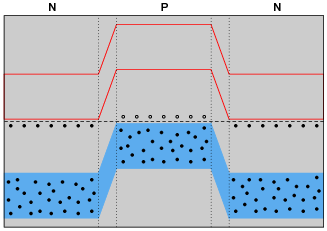
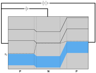
Question 11:
If we were to compare the energy diagrams for three pieces of semiconducting material, two "N" type and one "P" type, side-by-side, we would see something like this:
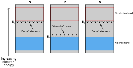
|
|
The presence of dopants in the semiconducting materials creates differences in the Fermi energy level (Ef) within each piece.
Draw a new energy diagram showing the equilibrium state of the three pieces after being joined together.
|
|
Notes:
If students are familiar with energy band diagrams for PN diode junctions, they should have no great difficulty drawing an energy diagram for an NPN junction.
Question 12:
Transistor operation may be explained in terms of three different currents: injection, diffusion, and collection. Describe what each of these currents are, and how they help explain the amplifying nature of a transistor.
Challenge question: explain how the relative doping concentrations of emitter, base, and collector regions is crucial in allowing a transistor to function as an amplifying device. What would happen to the collection current, for example, if the collector were as strongly doped as the emitter?
Notes:
As students research and use these terms in their study of bipolar junction transistors, the theory of BJT operation should become more evident. The terms really are well-chosen, accurately representing the motions of charge carriers within the transistor structure.
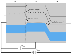
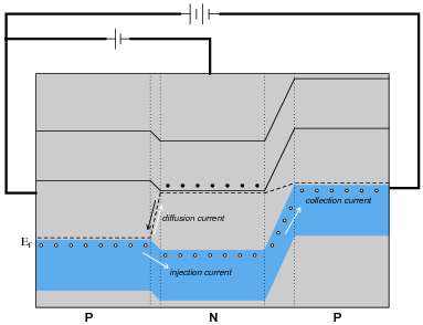
Question 13:
Trace the paths of injection, diffusion, and collection currents in this energy diagram for an NPN transistor as it is conducting:
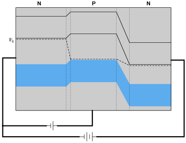
|
|
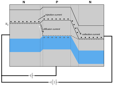
|
|
Notes:
A picture is worth a thousand words, they say. For me, this illustration is the one that finally made transistors make sense to me. By forward-biasing the emitter-base junction, minority carriers are injected into the base (electrons in the "P" type material, in the case of an NPN transistor), which then fall easily into the collector region. This energy diagram is invaluable for explaining why collector current can flow even when the base-collector junction is reverse biased.
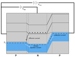
Question 14:
Trace the paths of injection, diffusion, and collection currents in this energy diagram for a PNP transistor as it is conducting:
|
|
|
|
Notes:
A picture is worth a thousand words, they say. For me, this illustration is the one that finally made transistors make sense to me. By forward-biasing the emitter-base junction, minority carriers are injected into the base (holes in the "N" type material, in the case of a PNP transistor), which then rise easily into the collector region. This energy diagram is invaluable for explaining why collector current can flow even when the base-collector junction is reverse biased.
When looking at energy diagrams, it is helpful to think of natural hole motion as air bubbles in a liquid, trying to rise as high as possible within their designated band.
Question 15:
From an examination of the energy diagram for a BJT in its conducting mode (current existing through each of the three terminals: emitter, base, and collector), determine the biasing of the two PN junctions:
- �
- The emitter-base junction (forward or reverse biased?)
- �
- The base-collector junction (forward or reverse biased?)
One of these two junctions actually operates in the reverse-bias mode while the transistor is conducting. Explain how this is possible, as a simple PN junction (a diode) operating in reverse-bias mode conducts negligible current.
Notes:
This question is possible to answer only if one understands the energy levels inside a BJT. The most common explanations of BJT function I find in introductory (non-engineering) textbooks completely omit discussions of energy levels, making the subject very confusing to new students.
Question 16:
Bipolar junction transistors are classified as minority carrier devices. Explain why.
Notes:
Note to your students that there is such a thing as a majority carrier type of transistor, but that it does not resemble the BJT in either construction or operational characteristics.
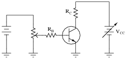
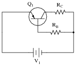
Question 17:
Transistors act as controlled current sources. That is, with a fixed control signal in, they tend to regulate the amount of current going through them. Design an experimental circuit to prove this tendency of transistors. In other words, how could you demonstrate this current-regulating behavior to be a fact?
|
|
Procedure: measure the voltage dropped across RC while varying VCC, for several different values of IB (inferred by measuring voltage drop across RB).
Notes:
Here, students must think like an experimental scientist: figuring out how to prove the relative stability of one variable despite variations in another, while holding the controlling variable constant. Encourage your students to actually build this circuit!
Question 18:
Compare the relative magnitudes of each current in this bipolar transistor circuit:
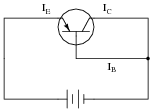
|
|
Which current is the smallest and which is the largest? Are there any two currents that are closer in magnitude than with the third? If so, which currents are they?
|
Notes:
Note the brief nature of the answer. This mathematical expression says it all, and it is a good review of inequality symbols.
Question 19:
Are the collector and emitter terminals of a transistor interchangeable? If not, what is the physical difference between the emitter and collector?
Notes:
Ask your students if there is any way to distinguish the emitter and collector terminals on a transistor, from external meter measurements. There is!
Question 20:
A beginning electronics student is just learning about transistors, and reads in the textbook that a bipolar transistor (either NPN or PNP) can be thought of as two diodes connected back-to-back as such:
|
|
Acting on this idea, the student proceeds to connect two 1N4001 rectifying diodes back-to-back and try to use it as a transistor. This idea does not work: although the diode pair reads the same patterns of continuity as a transistor would, it does not amplify. Explain why.
Note: this is a fairly deep question, and may not be answered without an understanding of charge carrier energy levels and semiconductor junction behavior.
Follow-up question: what do you suppose is really meant by the textbook's statement of bipolar transistors being equivalent to back-to-back diodes, if two diodes connected back-to-back do not exhibit amplifying behavior? Is this a completely wrong statement, or is there some truth to it?
Notes:
The idea for this question came from personal experience. I actually tried to build my own transistor out of two back-to-back diodes, and failed miserably. It took many years before I finally understood enough about semiconductor physics to realize why it would not work!
Question 21:
How would you explain the necessary conditions for conduction of an electric current through a BJT? Describe must be done to a BJT in order for it to conduct a current.
Notes:
This is perhaps the most important question your students could learn to answer when first studying BJTs. What, exactly, is necessary to turn one on? Have your students draw diagrams to illustrate their answers as they present in front of the class.
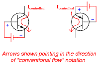
Question 22:
Draw the polarities (+ and -) of the applied voltages necessary to turn both these transistors on:
|
|
Also, draw the direction of the controlled current (flowing between collector and emitter) that will result from a power source properly connected between these terminals.
|
|
Follow-up question: draw the voltage sources necessary for generating the "controlled" current traced in these diagrams, so that the applied voltage polarity between collector and emitter is evident.
Notes:
This is a very important concept for students to grasp: how to turn a BJT on with an applied voltage between base and emitter, and also which direction the controlled current goes through it. Be sure to spend time discussing this, for it is fundamental to their understanding of BJT operation.
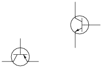
Question 23:
Students new to the study of transistors often have difficulty remembering the proper directions of currents through bipolar junction transistors, since there are three different currents (IB, IC, IE) and they must "mesh" through the transistor in a particular way.
Draw the proper current directions for each of these transistors, and explain how you are able to remember the correct directions they go:
|
|
|
|
Notes:
Rather than present a "rule of thumb" to use in remembering the proper current directions, I opt to let the students figure this out on their own. An important element of this should be the mathematics of BJT currents, primarily this equation:
|
This relationship, combined with Kirchhoff's Current Law, should provide all the help necessary to formulate a rule.
Question 24:
Predict how all three transistor currents (IB, IC, and IE) will be affected as a result of the following faults. Consider each fault independently (i.e. one at a time, no multiple faults):
|
|
- �
- Base resistor RB fails open:
- �
- Collector resistor RC fails open:
- �
- Solder bridge (short) past base resistor RB:
- �
- Solder bridge (short) past collector resistor RC:
For each of these conditions, explain why the resulting effects will occur.
- �
- Base resistor RB fails open: All three currents stop.
- �
- Collector resistor RC fails open: Base current unchanged, collector current stops, emitter current decreases to value of base current (IE = IB).
- �
- Solder bridge (short) past base resistor RB: All three currents greatly increase, transistor will likely overheat and fail.
- �
- Solder bridge (short) past collector resistor RC: Base current unchanged, collector current increases slightly (ideally will not change at all!), transistor dissipates more power in the form of heat (may overheat).:
Notes:
The purpose of this question is to approach the domain of circuit troubleshooting from a perspective of knowing what the fault is, rather than only knowing what the symptoms are. Although this is not necessarily a realistic perspective, it helps students build the foundational knowledge necessary to diagnose a faulted circuit from empirical data. Questions such as this should be followed (eventually) by other questions asking students to identify likely faults based on measurements.
Question 25:
Based on these DC continuity tester indications, what type of transistor is this, PNP or NPN?
- �
- Resistance with negative test lead on pin 1, positive test lead on pin 2: no continuity
- �
- Resistance with negative test lead on pin 1, positive test lead on pin 3: no continuity
- �
- Resistance with negative test lead on pin 2, positive test lead on pin 1: no continuity
- �
- Resistance with negative test lead on pin 2, positive test lead on pin 3: no continuity
- �
- Resistance with negative test lead on pin 3, positive test lead on pin 1: continuity
- �
- Resistance with negative test lead on pin 3, positive test lead on pin 2: continuity
Also, to the best of your ability, identify the transistor's three terminals (emitter, base, and collector).
Notes:
Advise your students about the risks of using an analog multimeter (in ohmmeter mode) to test semiconductor components. Some inexpensive analog multimeter designs actually switch the polarity of the test leads when in the ohmmeter mode. In other words, the red test lead actually connects to the negative side of the meter's internal battery, while the black test lead connects to the positive side of the internal battery! If you are used to associating red with positive and black with negative, this switch will be quite a surprise.
Ask your students: what effect would a switch in polarity such as the one just described have on the determination of a transistor's identity? What if the person thought their meter's red lead was positive and the black lead negative, when in fact it was just the opposite? Would this affect their ability to accurately identify the transistor's terminals? Why or why not?
Question 26:
Many digital multimeters have a "diode check" range that allows the user to measure the forward voltage drop of a PN junction:
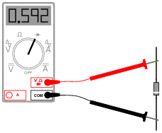
|
|
When using a multimeter with this feature to identify the terminals of a bipolar junction transistor, the forward voltage drop indication is necessary to distinguish the collector terminal from the emitter terminal. Explain how this distinction is made on the basis of the forward voltage measurement, and also explain why this is.
Notes:
I am surprised how many textbooks do not explain how to identify BJT terminals using a multimeter (especially a multimeter with the "diode check" function). This is a very important skill for technicians to have, as they will often be faced with transistor terminal identification in the absence of datasheets or other graphical references to device terminals.
Question 27:
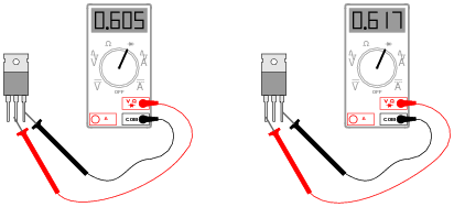
Identify the terminals on this BJT, and also the type of BJT it is (NPN or PNP):
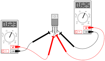
|
|
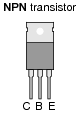
|
|
Notes:
I have found this "diode check" multimeter technique to be very successful for identifying BJT terminals.
Question 28:
One of the most important parameters for semiconductor components is the power rating. Explain why power rating is such a critical parameter, especially compared with other types of electronic components (resistors, inductors, capacitors, etc.).
Challenge question: some semiconductor datasheets specify altitude values (height above sea level) along with the power ratings. Explain why altitude has anything to do with the power rating of an electronic component.
Notes:
High temperature is the bane of most semiconductors. A classic example of this, though a bit dated, is the temperature sensitivity of the original germanium transistors. These devices were extremely sensitive to heat, and would fail rather quickly if allowed to overheat. Solid state design engineers had to be very careful in the techniques they used for transistor circuits to ensure their sensitive germanium transistors would not suffer from "thermal runaway" and destroy themselves.
Silicon is much more forgiving then germanium, but heat is still a problem with these devices. At the time of this writing (2004), there is promising developmental work on silicon carbide and gallium nitride transistor technology, which is able to function under much higher temperatures than silicon.