Bipolar junction transistors in active mode
Question 1:
| Don't just sit there! Build something!! |
Learning to mathematically analyze circuits requires much study and practice. Typically, students practice by working through lots of sample problems and checking their answers against those provided by the textbook or the instructor. While this is good, there is a much better way.
You will learn much more by actually building and analyzing real circuits, letting your test equipment provide the änswers" instead of a book or another person. For successful circuit-building exercises, follow these steps:
- 1.
- Carefully measure and record all component values prior to circuit construction, choosing resistor values high enough to make damage to any active components unlikely.
- 2.
- Draw the schematic diagram for the circuit to be analyzed.
- 3.
- Carefully build this circuit on a breadboard or other convenient medium.
- 4.
- Check the accuracy of the circuit's construction, following each wire to each connection point, and verifying these elements one-by-one on the diagram.
- 5.
- Mathematically analyze the circuit, solving for all voltage and current values.
- 6.
- Carefully measure all voltages and currents, to verify the accuracy of your analysis.
- 7.
- If there are any substantial errors (greater than a few percent), carefully check your circuit's construction against the diagram, then carefully re-calculate the values and re-measure.
When students are first learning about semiconductor devices, and are most likely to damage them by making improper connections in their circuits, I recommend they experiment with large, high-wattage components (1N4001 rectifying diodes, TO-220 or TO-3 case power transistors, etc.), and using dry-cell battery power sources rather than a benchtop power supply. This decreases the likelihood of component damage.
As usual, avoid very high and very low resistor values, to avoid measurement errors caused by meter "loading" (on the high end) and to avoid transistor burnout (on the low end). I recommend resistors between 1 kW and 100 kW.
One way you can save time and reduce the possibility of error is to begin with a very simple circuit and incrementally add components to increase its complexity after each analysis, rather than building a whole new circuit for each practice problem. Another time-saving technique is to re-use the same components in a variety of different circuit configurations. This way, you won't have to measure any component's value more than once.
Notes:
It has been my experience that students require much practice with circuit analysis to become proficient. To this end, instructors usually provide their students with lots of practice problems to work through, and provide answers for students to check their work against. While this approach makes students proficient in circuit theory, it fails to fully educate them.
Students don't just need mathematical practice. They also need real, hands-on practice building circuits and using test equipment. So, I suggest the following alternative approach: students should build their own "practice problems" with real components, and try to mathematically predict the various voltage and current values. This way, the mathematical theory "comes alive," and students gain practical proficiency they wouldn't gain merely by solving equations.
Another reason for following this method of practice is to teach students scientific method: the process of testing a hypothesis (in this case, mathematical predictions) by performing a real experiment. Students will also develop real troubleshooting skills as they occasionally make circuit construction errors.
Spend a few moments of time with your class to review some of the "rules" for building circuits before they begin. Discuss these issues with your students in the same Socratic manner you would normally discuss the worksheet questions, rather than simply telling them what they should and should not do. I never cease to be amazed at how poorly students grasp instructions when presented in a typical lecture (instructor monologue) format!
A note to those instructors who may complain about the "wasted" time required to have students build real circuits instead of just mathematically analyzing theoretical circuits:
What is the purpose of students taking your course?
If your students will be working with real circuits, then they should learn on real circuits whenever possible. If your goal is to educate theoretical physicists, then stick with abstract analysis, by all means! But most of us plan for our students to do something in the real world with the education we give them. The "wasted" time spent building real circuits will pay huge dividends when it comes time for them to apply their knowledge to practical problems.
Furthermore, having students build their own practice problems teaches them how to perform primary research, thus empowering them to continue their electrical/electronics education autonomously.
In most sciences, realistic experiments are much more difficult and expensive to set up than electrical circuits. Nuclear physics, biology, geology, and chemistry professors would just love to be able to have their students apply advanced mathematics to real experiments posing no safety hazard and costing less than a textbook. They can't, but you can. Exploit the convenience inherent to your science, and get those students of yours practicing their math on lots of real circuits!
Question 2:
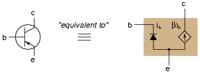
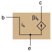
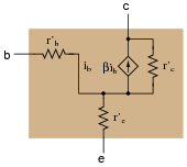
Models of complex electronic components are useful for circuit analysis, because they allow us to express the approximate behavior of the device in terms of ideal components with relatively simple mathematical behaviors. Transistors are a good example of components frequently modeled for the sake of amplifier circuit analysis:
|
|
It must be understood that models are never perfect replicas of the real thing. At some point, all models fail to precisely emulate the thing being modeled. The only real concern is how accurate we want our approximation to be: which characteristics of the component most concern us, and which do not.
For example, when analyzing the response of transistor amplifier circuits to small AC signals, it is often assumed that the transistor will be "biased" by a DC signal such that the base-emitter diode is always conducting. If this is the case, and all we are concerned with is how the transistor responds to AC signals, we may safely eliminate the diode junction from our transistor model:
|
|
However, even with the 0.7 volt (nominal) DC voltage drop absent from the model, there is still some impedance that an AC signal will encounter as it flows through the transistor. In fact, several distinct impedances exist within the transistor itself, customarily symbolized by resistors and lower-case r� designators:
|
|
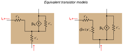
From the perspective of an AC current passing through the base-emitter junction of the transistor, explain why the following transistor models are equivalent:
|
|
|
|
The mathematical equivalence of these two expressions may be shown by factoring ib from all the terms in the left-hand model equation.
Notes:
The purpose of this question is to introduce students to the concept of BJT modeling, and also to familiarize them with some of the symbols and expressions commonly used in these models (as well as a bit of DC resistor network theory and algebra review, of course!).
Question 3:
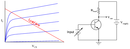
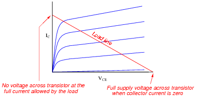
Load lines are useful tools for analyzing transistor amplifier circuits, but they may be hard to understand at first. To help you understand what "load lines" are useful for and how they are determined, I will apply one to this simple two-resistor circuit:
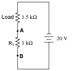
|
|
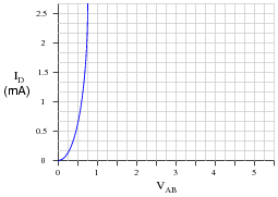
We will have to plot a load line for this simple two-resistor circuit along with the "characteristic curve" for resistor R1 in order to see the benefit of a load line. Load lines really only have meaning when superimposed with other plots. First, the characteristic curve for R1, defined as the voltage/current relationship between terminals A and B:
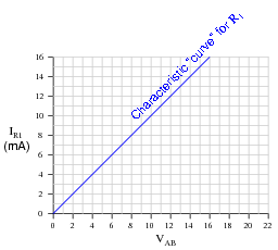
|
|
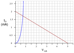
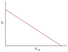
Next, I will plot the load line as defined by the 1.5 kW load resistor. This "load line" expresses the voltage available between the same two terminals (VAB) as a function of the load current, to account for voltage dropped across the load:
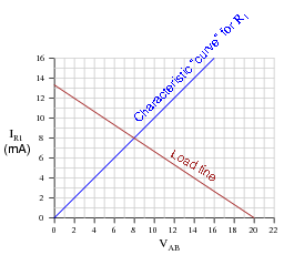
|
|
At what value of current (IR1) do the two lines intersect? Explain what is significant about this value of current.
Follow-up question: you might be wondering, "what is the point of plotting a 'characteristic curve' and a 'load line' in such a simple circuit, if all we had to do to solve for current was add the two resistances and divide that total resistance value into the total voltage?" Well, to be honest, there is no point in analyzing such a simple circuit in this manner, except to illustrate how load lines work. My follow-up question to you is this: where would plotting a load line actually be helpful in analyzing circuit behavior? Can you think of any modifications to this two-resistor circuit that would require load line analysis in order to solve for current?
Notes:
While this approach to circuit analysis may seem silly - using load lines to calculate the current in a two-resistor circuit - it demonstrates the principle of load lines in a context that should be obvious to students at this point in their study. Discuss with your students how the two lines are obtained (one for resistor R1 and the other plotting the voltage available to R1 based on the total source voltage and the load resistor's value).
Also, discuss the significance of the two line intersecting. Mathematically, what does the intersection of two graphs mean? What do the coordinate values of the intersection point represent in a system of simultaneous functions? How does this principle relate to an electronic circuit?
Question 4:
Load lines are useful tools for analyzing transistor amplifier circuits, but they may be applied to other types of circuits as well. Take for instance this diode-resistor circuit:
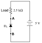
|
|
The diode's characteristic curve is already plotted on the following graph. Your task is to plot the load line for the circuit on the same graph, and note where the two lines intersect:
|
|
What is the practical significance of these two plots' intersection?
|
|
Follow-up question: explain why the use of a load line greatly simplifies the determination of circuit current in such a diode-resistor circuit.
Challenge question: suppose the resistor value were increased from 2.5 kW to 10 kW. What difference would this make in the load line plot, and in the intersection point between the two plots?
Notes:
While this approach to circuit analysis may seem silly - using load lines to calculate the current in a diode-resistor circuit - it demonstrates the principle of load lines in a context that should be obvious to students at this point in their study. Discuss with your students how the load line is obtained for this circuit, and why it is straight while the diode's characteristic curve is not.
Also, discuss the significance of the two line intersecting. Mathematically, what does the intersection of two graphs mean? What do the coordinate values of the intersection point represent in a system of simultaneous functions? How does this principle relate to an electronic circuit?
Question 5:
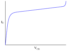
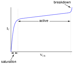
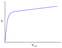
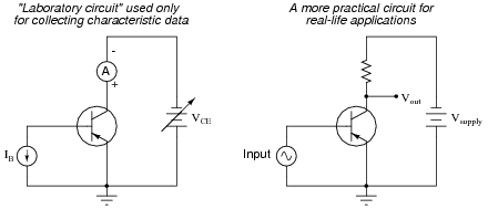
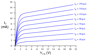
A very important measure of a transistor's behavior is its characteristic curves, a set of graphs showing collector current over a wide range of collector-emitter voltage drops, for a given amount of base current. The following plot is a typical curve for a bipolar transistor with a fixed value of base current:
|
|
A "test circuit" for collecting data to make this graph looks like this:
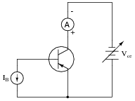
|
|
Identify three different regions on this graph: saturation, active, and breakdown, and explain what each of these terms mean. Also, identify which part of this curve the transistor acts most like a current-regulating device.
|
|
The transistor's best current-regulation behavior occurs in its äctive" region.
Follow-up question: what might the characteristic curves look like for a transistor that is failed shorted between its collector and emitter terminals? What about the curves for a transistor that is failed open?
Notes:
Ask your students what a perfect current-regulating curve would look like. How does this perfect curve compare with the characteristic curve shown in this question for a typical transistor?
A word of caution is in order: I do not recommend that a test circuit such as the one shown in the question be built for collecting curve data. If the transistor dissipates power for any substantial amount of time, it will heat up and its curves will change dramatically. Real transistor curves are generated by a piece of test equipment called a "curve tracer," which sweeps the collector-emitter voltage and steps the base current very rapidly (fast enough to "paint" all curves on an oscilloscope screen before the phosphor stops glowing).
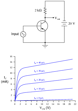
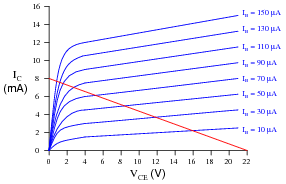
Question 6:
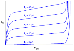
If a transistor is subjected to several different base currents, and the collector-emitter voltage (VCE) ßwept" through the full range for each of these base current values, data for an entire "family" of characteristic curves may be obtained and graphed:
|
|
What do these characteristic curves indicate about the base current's control over collector current? How are the two currents related?
Notes:
Ask your students what the characteristic curves would look like for a perfect transistor: one that was a perfect regulator of collector current over the full range of collector-emitter voltage.
Question 7:
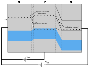
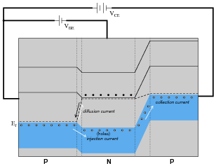
Conduction of an electric current through the collector terminal of a bipolar junction transistor requires that minority carriers be ïnjected" into the base region by a base-emitter current. Only after being injected into the base region may these charge carriers be swept toward the collector by the applied voltage between emitter and collector to constitute a collector current:
|
|
|
|
An analogy to help illustrate this is a person tossing flower petals into the air above their head, while a breeze carries the petals horizontally away from them. None of the flower petals may be ßwept" away by the breeze until the person releases them into the air, and the velocity of the breeze has no bearing on how many flower petals are swept away from the person, since they must be released from the person's grip before they can go anywhere.
By referencing either the energy diagram or the flower petal analogy, explain why the collector current for a BJT is strongly influenced by the base current and only weakly influenced by the collector-to-emitter voltage.
Notes:
This is one of my better analogies for explaining BJT operation, especially for illustrating the why IC is almost independent of VCE. It also helps to explain reverse recovery time for transistors: imagine how long it takes the air to clear of tossed flower petals after you stop tossing them, analogous to latent charge carriers having to be swept out of the base region by VCE after base current stops.
Question 8:
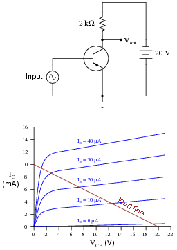
Determine the approximate amount of collector current for this transistor circuit, given the following characteristic curve set for the transistor:
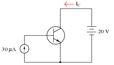
|
|
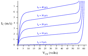
|
|
Follow-up question: how much will the collector current rise if the voltage source increases to 35 volts?
Notes:
This question is nothing more than an exercise in interpreting characteristic curves.
Question 9:
The following schematic diagram is of a simple curve tracer circuit, used to plot the current/voltage characteristics of different electronic components on an oscilloscope screen:
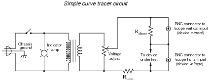
|
|
The way it works is by applying an AC voltage across the terminals of the device under test, outputting two different voltage signals to the oscilloscope. One signal, driving the horizontal axis of the oscilloscope, represents the voltage across the two terminals of the device. The other signal, driving the vertical axis of the oscilloscope, is the voltage dropped across the shunt resistor, representing current through the device. With the oscilloscope set for "X-Y" mode, the electron beam traces the device's characteristic curve.
For example, a simple resistor would generate this oscilloscope display:
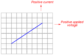
|
|
A resistor of greater value (more ohms of resistance) would generate a characteristic plot with a shallower slope, representing less current for the same amount of applied voltage:
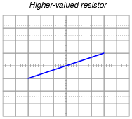
|
|
Curve tracer circuits find their real value in testing semiconductor components, whose voltage/current behaviors are nonlinear. Take for instance this characteristic curve for an ordinary rectifying diode:
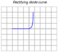
|
|
The trace is flat everywhere left of center where the applied voltage is negative, indicating no diode current when it is reverse-biased. To the right of center, though, the trace bends sharply upward, indicating exponential diode current with increasing applied voltage (forward-biased) just as the "diode equation" predicts.
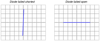
On the following grids, plot the characteristic curve for a diode that is failed shorted, and also for one that is failed open:
|
|
|
|
Notes:
Characteristic curves are not the easiest concept for some students to grasp, but they are incredibly informative. Not only can they illustrate the electrical behavior of a nonlinear device, but they can also be used to diagnose otherwise hard-to-measure faults. Letting students figure out what shorted and open curves look like is a good way to open their minds to this diagnostic tool, and to the nature of characteristic curves in general.
Although it is far from obvious, one of the oscilloscope channels will have to be ïnverted" in order for the characteristic curve to appear in the correct quadrant(s) of the display. Most dual-trace oscilloscopes have a "channel invert" function that works well for this purpose. If engaging the channel invert function on the oscilloscope flips the wrong axis, you may reverse the connections of the test device to the curve tracer circuit, flipping both axes simultaneously. Between reversing device connections and reversing one channel of the oscilloscope, you can get the curve to plot any way you want it to!
Question 10:
Explain why a bipolar junction transistor tends to regulate collector current over a wide range of collector-to-emitter voltage drops when its base current is constant. What happens internally that makes the BJT's collector current relatively independent of collector-to-emitter voltage and strongly dependent on base current?
Notes:
The current-regulating nature of a BJT is made more understandable by analyzing an energy band diagram of the transistor in active mode.
Question 11:
Many technical references will tell you that bipolar junction transistors (BJTs) are current-controlled devices: collector current is controlled by base current. This concept is reinforced by the notion of "beta" (b), the ratio between collector current and base current:
|
Students learning about bipolar transistors are often confused when they encounter datasheet specifications for transistor b ratios. Far from being a constant parameter, the "beta" ratio of a transistor may vary significantly over its operating range, in some cases exceeding an order of magnitude (ten times)!
Explain how this fact agrees or disagrees with the notion of BJTs being "current-controlled" devices. If collector current really is a direct function of base current, then why would the constant of proportionality between the two (b) change so much?
Follow-up question: if BJTs are not controlled by base current, then what are they controlled by? Express this in the form of an equation if possible. Hint: research the "diode equation" for clues.
Notes:
For discussion purposes, you might want to show your students this equation, accurate over a wide range of operating conditions for base-emitter voltages in excess of 100 mV:
|
This equation is nonlinear: increases in VBE do not produce proportional increases in IC. It is therefore much easier to think of BJT operation in terms of base and collector currents, the relationship between those two variables being more linear. Except when it isn't, of course. Such is the tradeoff between simplicity and accuracy. In an effort to make things simpler, we often end up making them wrong.
It should be noted here that although bipolar junction transistors aren't really current-controlled devices, they still may be considered to be (approximately) current-controlling devices. This is an important distinction that is easily lost in questions such as this when basic assumptions are challenged.
Question 12:
A common term used in semiconductor circuit engineering is small signal analysis. What, exactly, is ßmall signal" analysis, and how does it contrast with large signal analysis?
Follow-up question: why would engineers bother with two modes of analysis instead of just one (large signal), where the components' true (nonlinear) behavior is taken into account? Explain this in terms of network theorems and other mathematical "tools" available to engineers for circuit analysis.
Notes:
When researching engineering textbooks and other resources, these terms are quite often used without introduction, leaving many beginning students confused.
Question 13:
Explain what it means for a transistor to operate in its äctive" mode (as opposed to cutoff, saturation, or breakdown).
Notes:
Help your students contrast active transistor operation with what they know of transistors as switching elements (either saturated or cut off). Ask them to explain what is unique about transistor behavior in the active region that is not exhibited in any other region (i.e. the transistor's behavior with regard to collector current and collector-emitter voltage).
Question 14:
We know that graphs are nothing more than collections of individual points representing correlated data in a system. Here is a plot of a transistor's characteristic curve (for a single value of base current):
|
|
And here is a plot of the "load line" for a transistor amplifier circuit:
|
|
For each of these graphs, pick a single point along the curve (or line) and describe what that single point represents, in real-life terms. What does any single point of data along either of these graphs mean in a transistor circuit?
If a transistor's characteristic curve is superimposed with a load line on the same graph, what is the significance of those two plots' intersection?
For a load line, one point of data represents the amount of collector-emitter voltage available to the transistor for a given amount of collector current.
The intersection of a characteristic curve and a load line represents the one collector current (and corresponding VCE voltage drop) that will ßatisfy" all components' conditions.
Notes:
Discuss this question thoroughly with your students. So many students of electronics learn to plot load lines for amplifier circuits without ever really understanding why they must do so. Load line plots are very useful tools in amplifier circuit analysis, but the meaning of each curve/line must be well understood before it becomes useful as an instrument of understanding.
Ask your students which of the two types of graphs (characteristic curves, or load lines) represents a component's natural, or "free", behavior, and which one represents the bounded conditions within a particular circuit.
Question 15:
Describe what a load line is, at it appears superimposed on this graph of characteristic transistor curves:
|
|
What exactly does the load line represent in the circuit?
|
|
Follow-up question: why are load lines always straight, and not bent as the transistor characteristic curves are? What is it that ensures load line plots will always be linear functions?
Notes:
It is very important for students to grasp the ontological nature of load lines (i.e. what they are) if they are to use them frequently in transistor circuit analysis. This, sadly, is something often not grasped by students when they begin to study transistor circuits, and I place the blame squarely on textbooks (and instructors) who don't spend enough time introducing the concept.
My favorite way of teaching students about load lines is to have them plot load lines for non-transistor circuits, such as voltage dividers (with one of two resistors labeled as the "load," and the other resistor made variable) and diode-resistor circuits.
Question 16:
Though the characteristic curves for a transistor are usually generated in a circuit where base current is constant and the collector-emitter voltage (VCE) is varied, this is usually not how transistor amplifier circuits are constructed. Typically, the base current varies with the input signal, and the collector power supply is a fixed-voltage source:
|
|
The presence of a load resistor in the circuit adds another dynamic to the circuit's behavior. Explain what happens to the transistor's collector-emitter voltage (VCE) as the collector current increases (dropping more battery voltage across the load resistor), and qualitatively plot this load line on the same type of graph used for plotting transistor curves:
|
|
|
|
Notes:
Ask your student why this plot is straight, and not curved like the transistor's characteristic function.
Question 17:
Calculate and superimpose the load line for this circuit on top of the transistor's characteristic curves:
|
|
Then, determine the amount of collector current in the circuit at the following base current values:
- �
- IB = 10 mA
- �
- IB = 20 mA
- �
- IB = 30 mA
- �
- IB = 40 mA
|
|
- �
- IB = 10 mA ; IC = 3.75 mA
- �
- IB = 20 mA ; IC = 6.25 mA
- �
- IB = 30 mA ; IC = 8.5 mA
- �
- IB = 40 mA ; IC = 9.5 mA
Notes:
It would be good to point out something here: superimposing a linear function on a set of nonlinear functions and looking for the intersection points allows us to solve for multiple variables in a nonlinear mathematical system. Normally, only linear systems of equations are considered ßolvable" without resorting to very time-consuming arithmetic computations, but here we have a powerful (graphical) tool for approximating the values of variables in a nonlinear system. Since approximations are the best we can hope for in transistor circuits anyway, this is good enough!
Question 18:
In this graph you will see three different load lines plotted, representing three different values of load resistance in the amplifier circuit:
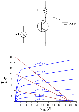
|
|
Which one of the three load lines represents the largest value of load resistance (Rload)? Which of the three load lines will result in the greatest amount of change in voltage drop across the transistor (DVCE) for any given amount of base current change (DIB)? What do these relationships indicate about the load resistor's effect on the amplifier circuit's voltage gain?
Notes:
This question challenges students to relate load resistor values to load lines, and both to the practical measure of voltage gain in a simple amplifier circuit. As an illustration, ask the students to analyze changes in the circuit for an input signal that varies between 5 mA and 10 mA for the three different load resistor values. The difference in DVCE should be very evident!
Question 19:
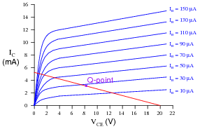
An important parameter of transistor amplifier circuits is the Q point, or quiescent operating point. The "Q point" of a transistor amplifier circuit will be a single point somewhere along its load line.
Describe what the "Q point" actually means for a transistor amplifier circuit, and how its value may be altered.
Notes:
Q points are very important in the design process of transistor amplifiers, but again students often seem to fail to grasp the actual meaning of the concept. Ask your students to explain how the load line formed by the load resistance, and characteristic curves of the transistor, describe all the possible operating conditions of collector current and VCE for that amplifier circuit. Then discuss how the status of that circuit is defined at any single point in time along those graphs (by a line, a curve, or a point?).
Question 20:
The following graph is a family of characteristic curves for a particular transistor:

|
|
Draw the load line and identify the Q-point on that load line for a common-collector amplifier circuit using this transistor:
|
|
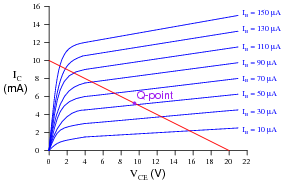
|
|
Follow-up question: the position of this circuit's Q-point is approximately mid-way along the load line. Would you say this is indicative of an amplifier biased for Class A operation, or for some other class of operation? Explain your answer.
Notes:
The purpose of this question is to get students to relate their existing knowledge of common-collector circuit DC analysis to the concept of load lines and Q-points. Ask your students to share their analysis techniques with the whole class.
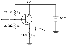
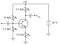
Question 21:
The following graph is a family of characteristic curves for a particular transistor:
|
|
Draw the load line and identify the Q-point on that load line for a common-emitter amplifier circuit using this transistor:
|
|
|
|
Follow-up question: determine what would happen to the Q-point if resistor R2 (the 2.2 kW biasing resistor) were to fail open.
Notes:
The purpose of this question is to get students to relate their existing knowledge of common-emitter circuit DC analysis to the concept of load lines and Q-points. Ask your students to share their analysis techniques with the whole class.
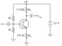
Question 22:
The following graph is a family of characteristic curves for a particular transistor:

|
|
Superimpose on that graph a load line for the following common-emitter amplifier circuit using the same transistor:
|
|
Also determine some bias resistor values (R1 and R2) that will cause the Q-point to rest approximately mid-way on the load line.
R1 = R2 =
|
|
There are several pairs of resistor values that will work adequately to position the Q-point at the center of the load line. I leave this an an exercise for you to work through and discuss with your classmates!
Follow-up question: determine what would happen to the Q-point if resistor R2 (the 2.2 kW biasing resistor) were to fail open.
Notes:
This is a very practical question, as technicians and engineers alike need to choose proper biasing so their amplifier circuits will operate in the intended class (A, in this case). There is more than one proper answer for the resistor values, so be sure to have your students share their solutions with the whole class so that many options may be explored.
Question 23:
Find one or two real bipolar junction transistors and bring them with you to class for discussion. Identify as much information as you can about your transistors prior to discussion:
- �
- Terminal identification (which terminal is base, emitter, collector)
- �
- Continuous power rating
- �
- Typical b
Notes:
The purpose of this question is to get students to kinesthetically interact with the subject matter. It may seem silly to have students engage in a ßhow and tell" exercise, but I have found that activities such as this greatly help some students. For those learners who are kinesthetic in nature, it is a great help to actually touch real components while they're learning about their function. Of course, this question also provides an excellent opportunity for them to practice interpreting component markings, use a multimeter, access datasheets, etc.