Class B BJT amplifiers
Question 1:
| Don't just sit there! Build something!! |
Learning to mathematically analyze circuits requires much study and practice. Typically, students practice by working through lots of sample problems and checking their answers against those provided by the textbook or the instructor. While this is good, there is a much better way.
You will learn much more by actually building and analyzing real circuits, letting your test equipment provide the änswers" instead of a book or another person. For successful circuit-building exercises, follow these steps:
- 1.
- Carefully measure and record all component values prior to circuit construction, choosing resistor values high enough to make damage to any active components unlikely.
- 2.
- Draw the schematic diagram for the circuit to be analyzed.
- 3.
- Carefully build this circuit on a breadboard or other convenient medium.
- 4.
- Check the accuracy of the circuit's construction, following each wire to each connection point, and verifying these elements one-by-one on the diagram.
- 5.
- Mathematically analyze the circuit, solving for all voltage and current values.
- 6.
- Carefully measure all voltages and currents, to verify the accuracy of your analysis.
- 7.
- If there are any substantial errors (greater than a few percent), carefully check your circuit's construction against the diagram, then carefully re-calculate the values and re-measure.
When students are first learning about semiconductor devices, and are most likely to damage them by making improper connections in their circuits, I recommend they experiment with large, high-wattage components (1N4001 rectifying diodes, TO-220 or TO-3 case power transistors, etc.), and using dry-cell battery power sources rather than a benchtop power supply. This decreases the likelihood of component damage.
As usual, avoid very high and very low resistor values, to avoid measurement errors caused by meter "loading" (on the high end) and to avoid transistor burnout (on the low end). I recommend resistors between 1 kW and 100 kW.
One way you can save time and reduce the possibility of error is to begin with a very simple circuit and incrementally add components to increase its complexity after each analysis, rather than building a whole new circuit for each practice problem. Another time-saving technique is to re-use the same components in a variety of different circuit configurations. This way, you won't have to measure any component's value more than once.
Notes:
It has been my experience that students require much practice with circuit analysis to become proficient. To this end, instructors usually provide their students with lots of practice problems to work through, and provide answers for students to check their work against. While this approach makes students proficient in circuit theory, it fails to fully educate them.
Students don't just need mathematical practice. They also need real, hands-on practice building circuits and using test equipment. So, I suggest the following alternative approach: students should build their own "practice problems" with real components, and try to mathematically predict the various voltage and current values. This way, the mathematical theory "comes alive," and students gain practical proficiency they wouldn't gain merely by solving equations.
Another reason for following this method of practice is to teach students scientific method: the process of testing a hypothesis (in this case, mathematical predictions) by performing a real experiment. Students will also develop real troubleshooting skills as they occasionally make circuit construction errors.
Spend a few moments of time with your class to review some of the "rules" for building circuits before they begin. Discuss these issues with your students in the same Socratic manner you would normally discuss the worksheet questions, rather than simply telling them what they should and should not do. I never cease to be amazed at how poorly students grasp instructions when presented in a typical lecture (instructor monologue) format!
A note to those instructors who may complain about the "wasted" time required to have students build real circuits instead of just mathematically analyzing theoretical circuits:
What is the purpose of students taking your course?
If your students will be working with real circuits, then they should learn on real circuits whenever possible. If your goal is to educate theoretical physicists, then stick with abstract analysis, by all means! But most of us plan for our students to do something in the real world with the education we give them. The "wasted" time spent building real circuits will pay huge dividends when it comes time for them to apply their knowledge to practical problems.
Furthermore, having students build their own practice problems teaches them how to perform primary research, thus empowering them to continue their electrical/electronics education autonomously.
In most sciences, realistic experiments are much more difficult and expensive to set up than electrical circuits. Nuclear physics, biology, geology, and chemistry professors would just love to be able to have their students apply advanced mathematics to real experiments posing no safety hazard and costing less than a textbook. They can't, but you can. Exploit the convenience inherent to your science, and get those students of yours practicing their math on lots of real circuits!
Question 2:
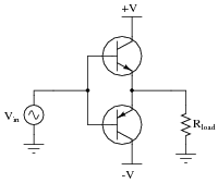
The circuit shown here is a standard push-pull amplifier, comprised of a complementary pair of bipolar junction transistors:
|
|
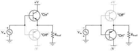
Trace current in this circuit during periods of time when the instantaneous voltage of the signal source (Vin) is positive, and for those periods when it is negative. Determine at which times each of the transistors is ön" (conducting current).
|
|
Follow-up question: would you classify this amplifier circuit as common-emitter, common-collector, or common-base? What kind of voltage gain would you expect this amplifier circuit to have?
Notes:
Have your students trace current in the circuit on a diagram drawn on the whiteboard, so all can see the analysis. After analyzing its operation, ask them why they think this amplifier is called "push-pull."
Another way to approach this circuit is from the perspective of current sourcing and current sinking. Which transistor sources current to the load resistor, and which transistor sinks current from the load resistor?
Question 3:
Class B amplifiers are greatly preferred over Class A designs for high-power applications such as audio power amplifiers. Explain why this is.
Notes:
Discuss why Class B amplifiers are more efficient than Class A amplifiers with your students. What is it about a Class A amplifier that makes it so inefficient for high-power applications?
Question 4:
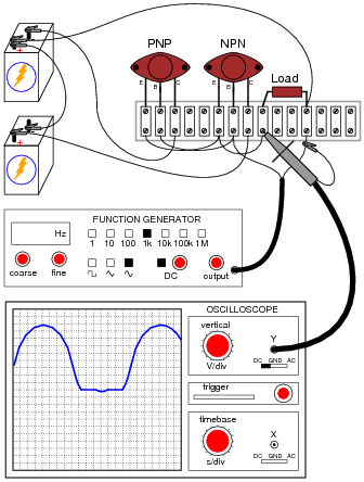
A student builds the following push-pull amplifier circuit, and notices that the output waveform is distorted from the original sine-wave shape output by the function generator:

|
|
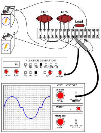
Thinking that perhaps this circuit requires DC biasing, just like Class A amplifier circuits, the student turns on the "DC offset" feature of the function generator and introduces some DC voltage to the input signal. The result is actually worse:
|
|
Obviously, the problem will not be fixed by biasing the AC input signal, so what causes this distortion in the output waveform?
Challenge question: since this type of transistor amplifier is often referred to as a "push-pull" design, describe the cause of this distortion in terms of the transistors "pushing" and "pulling".
Notes:
Crossover distortion is fairly easy to understand, but more difficult to fix than the one-sided "clipping" distortion students are used to seeing in Class A amplifier designs. If you think it might help your students understand better, ask them how a push-pull amplifier circuit would respond to a slowly changing DC input voltage: one that started negative, went to zero volts, then increased in the positive direction. Carefully monitor the transistors' status as this input signal slowly changes from negative to positive, and the reason for this form of distortion should be evident to all.
Question 5:
What would happen to the output voltage waveform of this amplifier if the NPN transistor failed open between collector and emitter?
|
|
|
|
Notes:
Ask your students to identify which transistor ßources" current to the load, and which transistor ßinks" current from the load, and the answer should be easy to understand.
Question 6:
A simple yet impractical way to eliminate crossover distortion in a Class B amplifier is to add two small voltage sources to the circuit like this:

|
|
Explain why this solution works to eliminate crossover distortion.
Also, explain what practical purpose this push-pull amplifier circuit might serve, since its voltage gain is only 1 (0 dB).
Such amplifier circuits are typically used as voltage buffers: effectively diminishing the output impedance of the source (boosting its current sourcing/sinking capability) so that it may supply more current to a load.
Challenge question: how would you estimate the output impedance of such an amplifier circuit?
Notes:
Ask your students to relate these bias voltage sources to the DC bias voltages previously seen in Class A amplifier designs. How much voltage do they think would be necessary to properly bias each transistor?
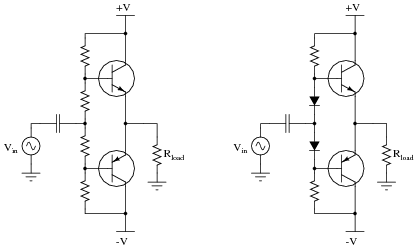
Question 7:
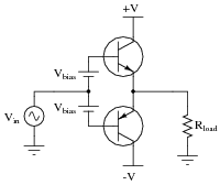
Two methods of biasing push-pull transistor pairs are shown here:
|
|
Which of these two methods is preferred, and why?
Notes:
Ask your students what is special about a diode that provides just the right amount of bias voltage for the transistors.
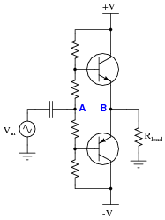
Question 8:
In a properly biased Class B amplifier circuit, how much voltage should be between the points A and B?
|
|
Follow-up questions: explain how this fact may be useful in troubleshooting push-pull amplifier circuits, and also explain how this fact proves the amplifier has a voltage gain of unity (1).
Notes:
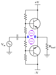
Challenge your students to apply Kirchhoff's Voltage Law to the "loops" around these two points, as such:
|
|
Knowing that the voltage between points A and B is zero, ask your students what the voltage drops must be across the biasing resistors. This question foreshadows the concept of a "virtual ground" in operational amplifier circuits. It is the idea that two or more points in a circuit may be held at the same potential without actually being connected together. In other words, the points are virtually common rather than being actually common with one another.
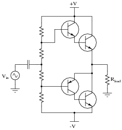
Question 9:
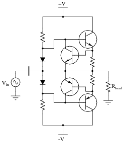
One way to greatly boost the current gain (AI) of a Class B push-pull amplifier is to use Darlington pairs instead of single transistors:
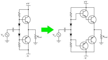
|
|
The only problem with the Darlington pair amplifier circuit shown is that the original biasing network will no longer be sufficient. Unless something else is changed in this circuit, the amplifier will exhibit some crossover distortion.
Draw the necessary modifications to the circuit to properly bias the new transistors, and explain why these modifications are necessary.
|
|
Notes:
Ask your students to estimate the additional biasing voltage necessary with the two (new) transistors added to the circuit. How much biasing voltage, per transistor, was necessary with just two transistors in the circuit? Now that four transistors are in the circuit, how much more biasing voltage is necessary to avoid crossover distortion?
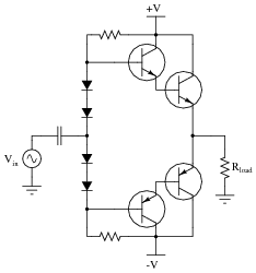
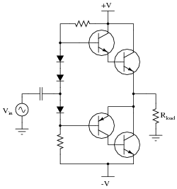
Question 10:
High-power PNP transistors tend to be scarcer and more expensive than high-power NPN transistors, a fact which complicates the construction of a high-power complementary push-pull amplifier circuits. An ingenious solution to this problem is to modify the basic Darlington push-pull circuit, replacing the final PNP transistor with an NPN transistor, like this:
|
|
The cascaded combination of an NPN and PNP transistor is called a Sziklai pair, or complementary Darlington pair. In this case, the small PNP transistor controls the larger NPN power transistor in the Sziklai pair, performing the same basic function as a PNP Darlington pair.
Modify the circuit shown here to use diodes in the biasing network instead of just resistors. The solution is not quite the same for this circuit as it is for a conventional Darlington push-pull circuit!
|
|
Notes:
Discuss the difference between the two halves of this amplifier circuit (the upper Darlington half, and the lower Sziklai half), paying special attention to the number of PN junctions between base and (final) emitter terminals.
Question 11:
A popular variation of the Class B amplifier is the Class AB amplifier, designed to eliminate any trace of crossover distortion. What makes the difference between a Class B and a Class AB amplifier? Why do Class AB amplifiers have less crossover distortion than Class B amplifiers? And, is there any disadvantage to changing from Class B to Class AB operation?
Amplifiers operating in Class AB mode are less power-efficient than pure Class B operation.
Notes:
Ask your students to specifically identify the change(s) that would have to be made in the following Class B circuit to make it operate as a Class AB amplifier:
|
|
Discuss why the name "Class AB" is given to this mode of operation. How does Class AB operation differ from pure Class A or pure Class B?
Question 12:
An interesting addition to the basic Class B push-pull amplifier circuit is overcurrent protection, in the form of two more transistors and two more resistors added to the circuit:
|
|
This form of overcurrent protection is common in voltage-regulated DC power supply circuitry, but it works well in amplifier circuitry, too. Explain how the additional transistors and resistors work together to protect the main power transistors from damage in the event of an overload.
Challenge question: what mathematical procedure would you use to size the emitter resistors? How much resistance is appropriate in this application?
Notes:
If students are having difficulty understanding how this circuitry works, it might be worthwhile to show them this circuit (from a regulated DC power supply):
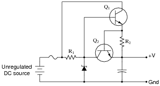
|
|
Ask them how transistor Q2 in this circuit works to protect transistor Q1 from overload.
An interesting way to explain the operation of this form of overcurrent protection is to say that when the auxiliary transistor begins to conduct (shorting base current away from the main power transistor), it effectively decreases the b of the main power transistor. By suddenly making the main power transistor less effective at amplifying, the signal source "feels" more of the load. This causes the signal source's voltage to sag, ultimately limiting load current in the process.